In accordance with an aspect of the invention, a non-volatile memory such as a multi-bit-per-cell flash memory includes multiple memory arrays or banks with each memory bank containing multiple sectors with reference cells and storage cells. Before first writing data to a sector in a memory bank after erasing the sector, the values that a single memory cell can store are written into a set of reference cells in the sector. For example, when each memory cell can store an N-bit value, there are at least one set of 2N reference cells per sector, and values 0 to 2N -1 are written in 2N reference cells when first writing to a sector. Alternatively, the reference values can be written to reference cells after writing data or in an interleaved fashion while writing data.
A read circuit for the memory includes a threshold voltage (Vt) read circuit, a content addressable memory, and an encoder. The Vt read circuit has a range of digital output values that is equal to or greater than the range of digital values that can be stored in a memory cell. For example, if each memory cell can store an N-bit value, the Vt read circuit reads out digital values having N+M bits where M is equal to or greater than zero. When reading from a sector, the Vt read circuit first reads from the reference cells in the sector and writes the N+M-bit values to the content addressable memory. The Vt read circuit then reads a storage cell and applies an N+M-bit value to the content addressable memory. The matching one of the 2n values in the content addressable memory identifies the stored value, and the encoder outputs a digital value according to which reference value in the content addressable memory matches the value that the Vt read circuit read. From one read operation to the next, the output values of the Vt read circuit can change because of changes in temperature, supply voltage, disturb and charge leakage of cells in the array, and endurance history, for example. However, since the reference cells are identical to the storage cells and written at approximately the same time, the variations of values read from reference and storage cells track each other so that the output data is independent of the variations.
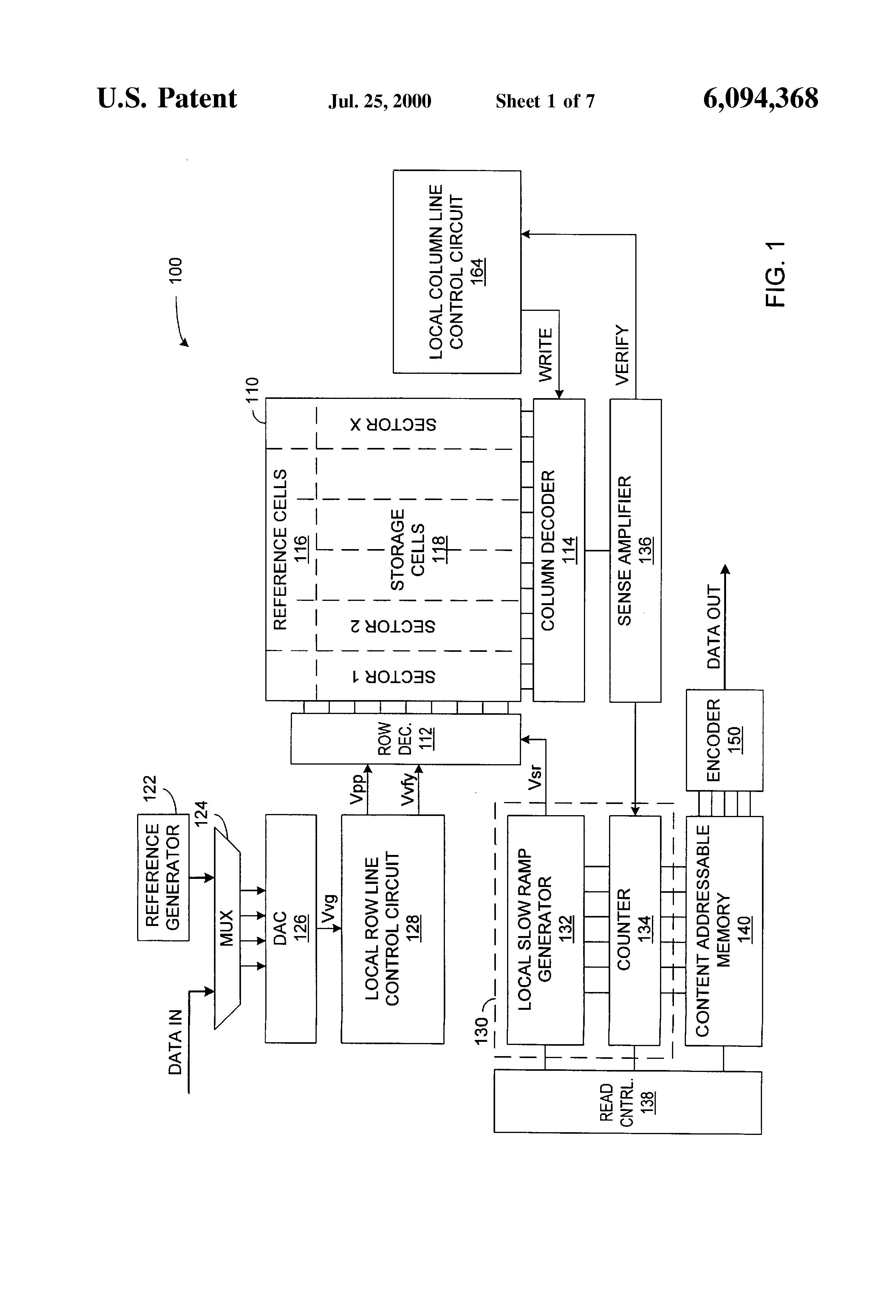
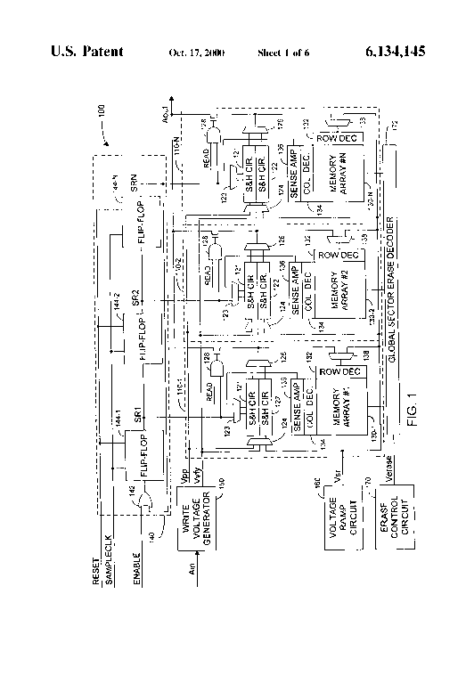
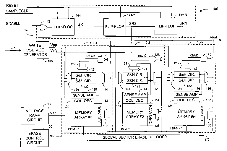
FIG. 1 is a block diagram of a portion of a multi-bit-per-cell memory 100 having autotracking in accordance with an embodiment of the invention. Memory 100 includes multiple memory arrays or banks 110 of memory cells, but for ease of illustration FIG. 1 shows only one memory bank 110. In an exemplary embodiment, memory 100 includes 64 memory banks 110 that are adapted for pipelined read and write operations such as described in U.S. Pat. No. 5,680,341, entitled "Pipelined Record and Playback for Analog Non-Volatile Memory"; U.S. Pat. No. 5,969,986, entitled "High-Bandwidth Read and Write Architectures for Non-Volatile Memories"; and U.S. patent application Ser. No. 09/128,225, entitled "High Data Rate Write Process for Non-Volatile Flash Memories" which are hereby incorporated by reference herein in their entirety. Each memory bank 110 is an array of multi-bit-per-cell memory cells such as an array of floating stacked-gate or split-gate floating gate Flash memory cells wherein a programmable threshold voltage of each memory cell represents an N-bit value. Alternatively, other types of multi-bit-per-cell memory cells such as EEPROM or DRAM cells might be employed. In an exemplary embodiment, each memory cell stores a 4-bit value, and the values that can be stored in a single memory cell are 0 to 15. Each memory cell in bank 110 is either a reference cell 116 or a storage cell 118. (Although FIG. 1 shows reference cells 116 at an edge of array 110, reference cells 116 can be located in array 110 and can be dispersed among storage cells 118.) Reference cells 116 and storage cells 118 have the same structure but different uses. Storage cells 118 store data with one N-bit data value per storage cell. Reference cells 116 store reference values that represent the N-bit data values. An autotracking read process uses reference cells 116 as described further below when reading data from a storage cell 118.
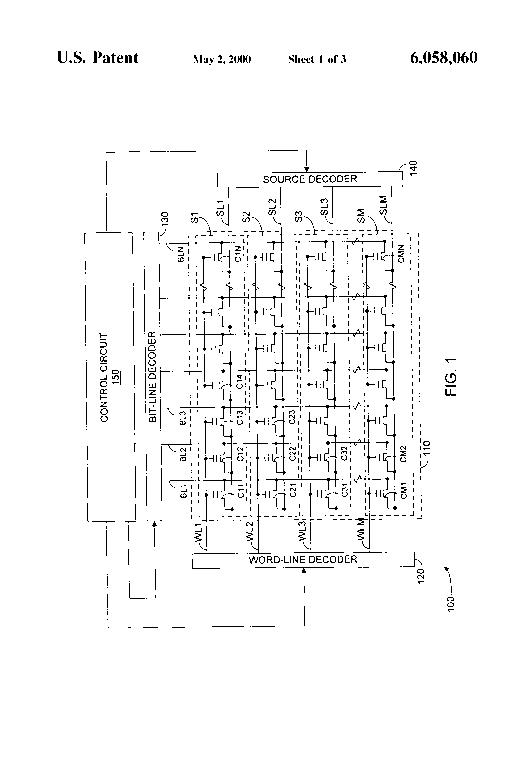
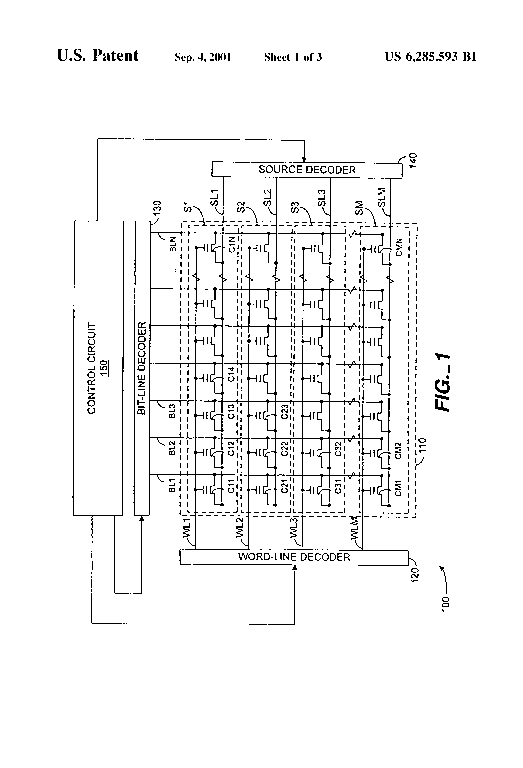
Memory bank 110 has a Flash array architecture and includes one or more erasable sectors. In the exemplary embodiment of the invention, each sector includes eight columns of memory cells. To erase a sector in array 110, a row decoder 112 grounds the row lines of bank 110, a column decoder 114 causes the column lines of the sector to float, and a local charge pump 162 charges a source line for the sector to an erase voltage Verase (typically about 10-12 volts). Alternatively, a negative-gate erase process applies a negative control gate voltage of about -8 to -10 volts while the source line for the sector being erased is at +5 to +6 volts. After an erase, a sector can be prepared for writing of data by first writing a set of reference values to the reference cells 116 in the sector. The reference values written include each of the values from the range of digital values that can be stored in one of storage cells 118. For example, a sector initialization process writes values 0 to 15 to sixteen reference cells in the exemplary embodiment. More reference cells are required for memories storing more bits per memory cell. For example, an 8-bit-per-cell memory uses 256 memory cells to store values 0 to 255. Since the exemplary embodiment includes eight columns of memory cells per sector, two rows of memory cells and two row lines of array 110 are dedicated to provide sixteen reference cells 116. The row lines dedicated to reference cells 116 are outside the user addressing scheme for storage cells 118. Reference cells 116 accordingly do not have addresses in the address space for data but have row lines that a row decoder 112 selects when a read control circuit 138 indicates an access of reference cells 116. Immediately after the reference values are written to reference cells 116 in a sector, data can be written to the storage cells 118 of the sector.
Write circuitry for memory bank 110 including a digital-to-analog converter (DAC) 126, a local row line control circuit 128, and a local charge pump writes the reference values in reference cells 116 and data in the storage cells 118. For the reference values, a reference generator 122 generates the series of digital reference values, and an input multiplexer 124 selects digital reference values for writing. In the write process, DAC 126 converts the digital values from multiplexer 124 to a global verify voltage Vvg that depends on the multi-bit value being written. Global verify voltage Vvg identifies the target threshold voltage to be written to a memory cell. In one embodiment of the invention, DAC 126 provides global verify voltage Vvg with a voltage level (typically between about 2 and 6 volts) that is within the threshold voltage range of the memory cells. DAC 126 can be implemented as a conventional linear DAC with a level shifter that shifts the output signal Vvg to an appropriate level indicating a target threshold voltage to be written. Alternatively, DAC 126 can perform a non-linear conversion, for example, such that high target threshold voltages are more widely separated than are the lower target threshold voltages. Additionally, DAC 126 can implement a conversion including Grey coding such that any two consecutive verify voltages Vvg from DAC 126 correspond to digital values that differ in only a single bit and are not necessarily consecutive digital values.
In accordance with another aspect of the invention, DAC 126 can implement several alternative conversions from digital input values to output global verify voltages Vgv, and DAC 126 can switch from one conversion to another each time a sector is erased This has the advantage of changing the threshold voltage associated with each data value. As described further below, reference cells 116 have location associated with multi-bit digital values and in some embodiments of the invention, are always programmed to the threshold voltage corresponding to the associated multi-bit digital value. Writing the same high (or low) threshold to the same reference can lead to endurance problems and can change the characteristics of some reference cells 116. Changing the conversion of DAC 126 changes the threshold voltages written to reference cells 116 and reduces the endurance problem. Alternatively, as described further below, the locations of reference cells 116 can change, rotate, or shift every write cycle.
Local row line control circuit 128 generates write voltages Vpp Vvfy that row decoder 112 applies the row line coupled to a programmed. The verify voltage Vvfy is typically the same as the global verify voltage Vvg that generator 128 samples when directed to begin a write operation. Row decoder 112 applies write voltage Vpp (typically between about 6 and 12 volts) to the selected row line during a series of programming pulses and applies verify voltage Vvfy to the selected row line during a series of verify cycles. Row decoder 112 grounds the unselected row lines for both programming pulses and verify cycles. During the programming pulses, column decoder 114 applies a programming voltage Vw (typically between about 4 and 6 volts) from the charge pump to the selected column line associated with the memory cell being programmed. The combination of the row line programming voltage Vpp on the control gate (or row line) of the selected memory cell, the column line programming voltage Vw on the drain (or column line) of the selected memory cell, and the grounded source of the selected memory cell causes channel hot electron injection that injects electrons into the floating gate of the selected memory cell. Accordingly, the threshold voltage of the selected memory cell rises during each programming pulse.
During each verify cycle, row decoder 112 applies verify voltage Vvfy to the control gate of the selected memory cell, and column decoder 114 applies a read voltage Vr (typically about 1 volt) to the selected column line and connects a sense amplifier 136 to the selected column line. If the threshold voltage of the selected memory cell is below the target level (i.e., below verify voltage Vvfy), the selected memory cell conducts during the verify cycle, and sense amplifier 136 asserts a signal indicating that programming pulses should continue. When a programming pulse raises the threshold voltage of the selected memory cell to or above the target threshold voltage that verify voltage Vvfy indicates, the selected memory does not conduct during the following verify cycle, and sense amplifier 136 asserts a signal to stop further programming pulses.
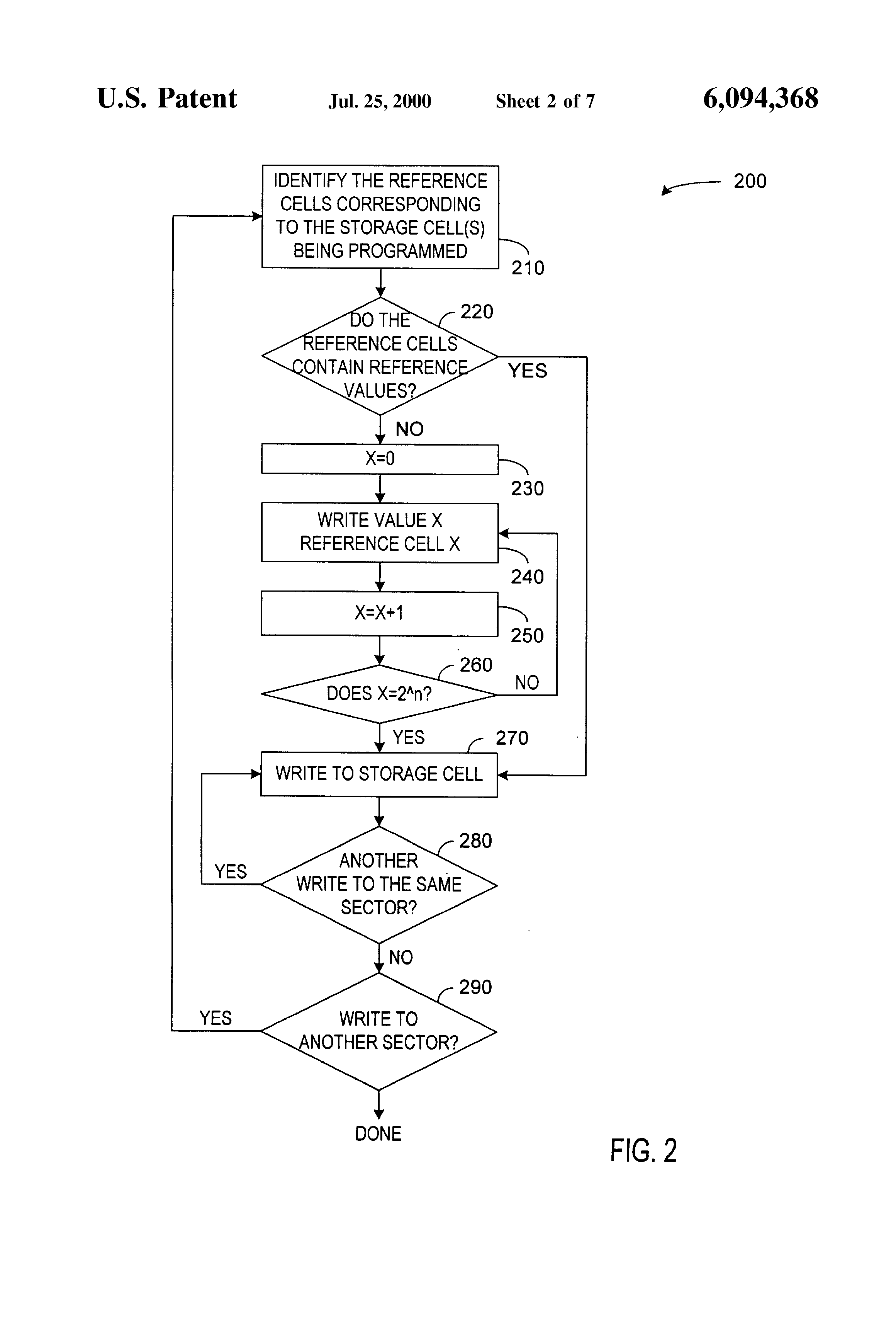
FIG. 2 is a flow diagram of a write process 200 in accordance with an embodiment of the invention. In an initial step 210, write process 200 identifies the reference cells associated with the storage cell or cell being written. In the exemplary embodiment of the invention, each sector of an array includes a set of 2n reference cells 116. In a typical Flash memory where a sector contains 32K or 64K storage cells 118, sixteen reference cells 116 for a 4-bit-per-cell memory is a small fraction of the total number of memory cells, and timing overhead for use of reference cells 116 is also small. However, to reduce the number of reference cells 116, an entire array may include only a single set of 2n reference cells, or memory 100 may include only one set of reference cells per Vt read circuit. Fewer reference cells may be sufficient because often variations in the output values from the Vt read circuit are associated with the Vt read circuit or common to an entire array, not a specific sector. Alternatively, each sector can include more than one set of reference cells 116 with each set of reference cells being associated with a particular portion of the sector containing the reference cells. Having more reference cells allows the physical locations of reference cell 116 to be closer to the associated storage cells 118 and allows the write times of reference values to be closer to the write times of the data values. Accordingly, with more reference cells 116, the reference cells 116 may better track the behavior of associated storage cells 118.
Step 220 determines whether the reference cells 116 associated with the storage cells 118 being read contain reference values. Write process 200 is best employed in a system for storage of block of data where a block of data is sequentially written to a sector. An example of such a system is a record and playback system that records an analog signal such as a sound or video signal as a series of digital sample. Another example is a digital mass data storage device such as a Flash memory card. In such a system, a sector including reference and storage cells is erased, before write process 200 begins, and step 220, which checks whether the reference cells contain reference values, is not required. The sector starts erased and is filled with reference and data values without intervening writes to other sectors. However, write process 200 can be more generally applied to random access writing where writing of values can move from sector to sector.
For the first time data is written to a sector after an erase of the sector, the reference cells 116 are in the erased state and do not contain reference values. Multiplexer 124 selects reference generator 122 as the source of reference values to be written. Step 230 and a loop including steps 240, 250, and 260 write the reference values in the reference cells 116 identified in step 210. In step 230, reference generator 122 initializes an index X for the sequential generation of consecutive digital values starting at zero. Alternatively, generation of reference values can be in any desired order provided that each value is written to the reference cell associated with the value. Step 240 writes value X to the reference cells 116 that associated with value X. In step 250, reference generator 122 increments index X before determining in step 260 whether the last reference value has been written to the last reference cell.
After writing the reference values, multiplexer 124 selects an input data signal DATA-- IN as the source of data values written to storage cells 118. Data values are written to storage cells 118 using the same write process and write circuitry that write to reference cells 116. A step 270, which writes a multi-bit data value to a storage cell 118, is repeated as long as there are new data values to be written in the same sector. For a write operation writing an entire sector of 32K or 64K storage cells 118, the writing of reference values in reference cells 116 provides a minimal performance penalty. For a random access write of a data value, process 200 moves back to the initial step 210 of identifying the reference cells for the data value to be written if the data value to be written is not in the same sector as the data value last written to a storage cell 118. If reference values for the storage cell were previously written to the reference cells in the newly identified sector, the reference values do not need to be written.
Returning to FIG. 1, memory 100 includes a digital Vt read circuit 130, a content addressable memory 140, an encoder 150, and a read control circuit 138 that controls the read process. Digital Vt read circuit 130 can be any known read circuit that is capable reading the threshold voltage of a selected memory cell and generating a multi-bit digital value that corresponds to the threshold voltage of the selected memory cell. Further, in accordance with an aspect of the invention, the multi-bit digital value from Vt read circuit 130 includes more bits than do the values stored in the storage cells 118. For example, in the exemplary embodiment where each storage cell 118 stores a 4-bit data value, Vt read circuit 130 provides a 5-bit or 6-bit value indicating the threshold voltage read from a memory cell.
In FIG. 1, Vt read circuit 130 includes a local slow ramp generator 132 and a counter 134 which are coupled to row decoder 112 and sense amplifier 136. U.S. patent application Ser. No. 09/053,716, entitled "High Resolution Multi-Bit-Per-Cell Memory", filed Apr. 8, 1998, describes other suitable read circuits and is hereby incorporated by reference in its entirety. Slow ramp generator 132 generates a signal Vsr. which row decoder 112 applies to the control gate of the memory cell selected for a read (i.e., to the selected row line). Signal Vsr slowly changes voltage to cross the range of possible threshold voltages for memory cells. For reading the threshold voltage, counter 134 counts periods of a clock signal as signal Vsr moves across the threshold voltage range. When signal Vsr reaches the threshold voltage of the selected memory cell, sense amplifier 136 senses a change in the conductivity of the selected memory cell and stops counter 134 from counting further. The count from counter 134 provides a digital value indicating the threshold voltage of the selected memory cell.
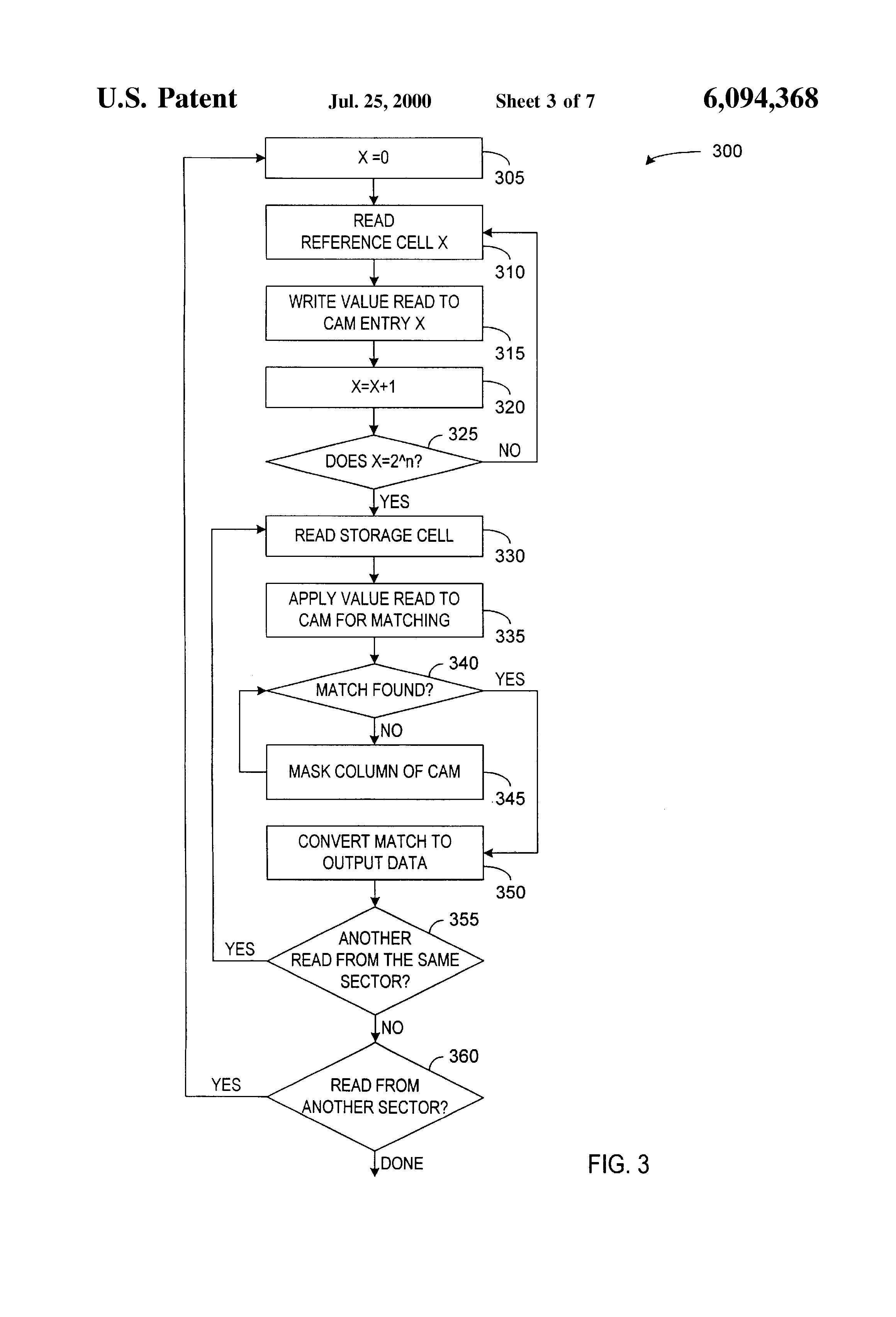
FIG. 3 is a flow diagram of an autotracking read process 300 in accordance with an embodiment of the invention. Process 300 starts in step 305 by initializing an index X for the address or location of the first reference cell 116 in a sector containing data to be read. Steps 310 and 315 respectively read the threshold voltage of the reference cell 116 that corresponds to index X and write the digital value read to a corresponding entry (or word) X in content addressable memory 140. After writing the digital value to CAM 140, step 320 increments index X, and a step 325 determines whether all of the reference values have been read. If not, steps 310 and 315 are repeated to read the reference cell 116 corresponding to the next value of index X. After a digital reference value from the last reference cell 116 in the sector has been written into the appropriate entry of CAM 140, process 300 transitions from step 325 to start reading storage cells 118.
Step 330 reads the selected storage cell 118 using Vt read circuit 130, and step 335 applies the value read to the CAM 140 for a match operation that locates an entry of CAM 140 containing a matching reference value. Typically, the value read from the storage cell 118 matches one of values in the entries of CAM. If there is a match, process 300 branches from decision step 340 to step 350 where encoder 150 generates the output data value. The output data has a value that corresponds to or identifies the entry of CAM 140 containing the matching value. Since Vt read circuit 140 provides digital values containing more bits than do the stored data, the value read may not exactly match any of the values in CAM 140. In this case, step 345 turns off or masks out a column of CAM 140 corresponding to the least significant bit of value read and the values stored in CAM 140. CAM 140 tests for a match in step 340. If no match is found again, step 345 turns off or masks out another column or bit of CAM 140 and continues turning off columns until a match is found or a data error is identified.
If another storage cell 118 in the same sector is to be read, the storage cell can be read without changing the content of CAM 140. Process 300 branches from a decision step 355 back to step 330 and reads another storage cell 118 from the current sector. Thus, when reading an entire sector, reading of the reference cells 116 minimally affects read performance. If the next storage cell 118 to be read is in another sector, read process 300 branches from a decision step 360 back to step 305 to read the reference cells from the new sector being accessed and reload CAM 140.
In embodiments of the invention having one set of reference cells per array 110, CAM 140 is reloaded only if the same Vt read circuit reads from the new array. Preferably, each array 110 has corresponding local read circuitry including a Vt read circuit and CAM 140, and the CAMs 140 are only loaded once per array. CAMs 140 can also be periodically loaded or refreshed if operating parameters may change during operation of a memory 100. For example, a match operation that fails to find a match in CAM 140 may signal a change in operating parameters. In response to a match operation failing to find a match, the reference cells 116 can be read and values read from reference cells 116 written to the associated CAM 140 before another match operation attempts to match the value read from a storage cell to the value from a reference cell 116.
Table 1 illustrates the variation in the content of CAM 140 for the exemplary embodiment of memory 100 where each storage cell stores four bits of data and the Vt read circuit provides a 6-bit digital signal. The variations of Table 1 are due to the clock signal for counter 134 having different frequencies, while the voltage of signal Vsr ramps at a constant rate independent of the clock signal's frequency. As illustrated in Table 1, variation in the frequency varies the count that the Vt read circuit reads for a reference cell or a storage cell. For example, when the Vt read circuit reads a storage cell 118 into which the value 8 was written, the count is 16 if the clock signal has the correct frequency f, if the clock signal is 25% fast, or 12 if the clock signal is 25% slow. However, the count read from a storage cell 118 when applied to CAM 140 matches the entry (or word) 8 for any of the clock frequencies. Other variations in the operating parameters and device characteristics of memory 100 can have similar effects on the value output from the Vt read circuit, but the final data output value from encoder 150 is independent of such variations.
Table 1 also includes a column for the look-up value which indicates the output data value from encoder 150 when the value read from a storage cell matches the content of the associated CAM entry.
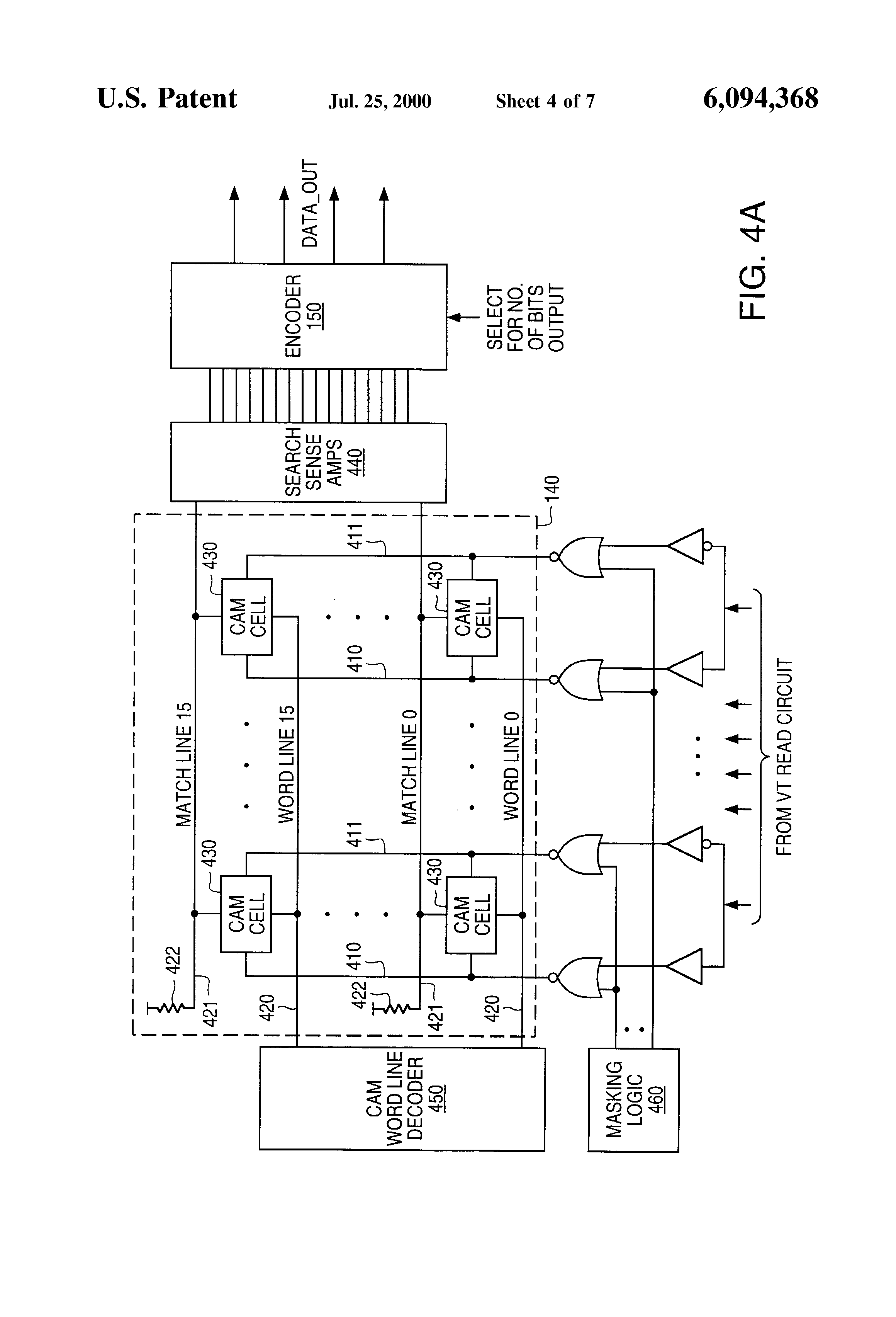
FIG. 4A illustrates an example of CAM 140 including sixteen rows of CAM cells 430. The embodiment of CAM 140 of FIGS. 4A and 4B is merely one example of an SRAM based binary CAM. Alternative CAM include but are not limited to ternary CAM (having a "don't care" state) or non-volatile Flash CAM. As shown in FIG. 4B, each CAM cell 430 has a pair of nodes NA and NB which are between respective pull-up transistors 431A and 431B and respective pull- down transistors 432A and 432B. The gates of transistors 431A and 432A are coupled to node NB, and the gates of transistors 431B and 432B are coupled to node NA. Pass transistors 433A and 433B in each CAM cell connect respective node NA and NB to respective bit lines 410 and 411 associated with a bit corresponding to the CAM cell 430. Pass transistors 433A and 433B have gates coupled to a word line 420 associated with a row including the CAM cell.
Each row of CAM 140 corresponds to an entries or word and includes N+M CAM cells. A write operation sets the polarity of the nodes NA in the CAM cells of an entry to the same binary states as a digital signal applied to the associated bit line 410. A binary signal on the complementary bit line 411 has the opposite binary state from the signal on bit line 410, and node NB has a binary state opposite that of node NA. ( Bit lines 410 and 411 connect to the Vt read circuit through masking logic 460.) During a write to CAM 140, a digital signals (and its binary complement) representing a N+M-bit value to be written to CAM 140 is asserted to bit lines 410 (and 411), and a word line 420 corresponding to the entry being written is asserted. Pass transistors 435 and 436, which have gates coupled to the associated word line 420, connect respective nodes NA and NB to associated complementary bit lines 410 and 411. Each node NA charges to the state associated a bit being written to the CAM cell 430 before the signal on the selected word line 420 is deasserted. Pull-up transistors 431 and 432 and pull-down transistors 433 and 434 preserve the states of nodes NA and NB in each CAM cell after the associated word line is deasserted.
CAM 140 also includes match lines 421 where each match line 421 is associated with and coupled to the CAM cells 430 that forms an associated entry. Each match line 421 has a pull-up-resistor 422 which connects the match line 421 to a voltage such as supply voltage Vcc. In each CAM cell 430, transistors 435A and 434B in series and transistors 435B and 434A in series connect the associated match line 421 to ground. Transistors 434A and 434B have gates coupled to respective nodes NA and NB so that only the one of transistors 434A or 434B that corresponds to the node NA or NB in the high binary state conducts. For a match operation, binary signals representing the value to be matched are applied to bit lines 410 and 411. Transistors 435A and 435B have gates coupled to bit lines 410 and 411 respectively. A CAM cell 430 pulls down the associated match line 421 if both transistors 435A and 434B conduct or both transistors 435B and 434A conduct. This occurs when the bit represented on associated bit lines 410 and 411 does not correspond to the binary states of the nodes NA and NB in the CAM cell. Accordingly, if all of the input bits match the bits stored in the CAM cell of an entry, the match line 421 remains at high voltage. Sense amps 440 sense match lines 421 and assert a signal indicate which if any of the CAM entries stores a word matching the input data signal. Masking logic 460 can turn off or mask a column of CAM cells 430 during a match operation so that a match line 421 remaining high indicates that an input value matches all of the bits corresponding to columns that are not masked.
Encoder 150, which connects to sense amplifiers 440 of CAM 140, generates an N-bit digital output signal DATA-- OUT identifying which of the match lines indicates a match. Data output signal DATA-- OUT is independent of the variations in memory 100 for the reasons indicated above. In the embodiment of FIG. 4, encoder 150 is a look-up table that generates an N-bit digital output signal DATA-- OUT. Such look-up tables can be implemented in hardwired logic gates, binary mask ROM, or re-writeable memory cells such as Flash memory cells or SRAM cells. With a re-writeable look-up table, the mapping between entries of CAM 140 and output data values can change. The mapping can reduce the number of output of bits per memory cell, for example, by mapping two or more entries to the same output data values. A signal can also select number of bits output from encoder 150 by causing encoder 150 to drop one or more of the bits that would otherwise be output.
A re-writeable look-up table in encoder 150 can also be change according to a user-provided encryption key for data decryption. FIG. 6 illustrates a memory 600 including data encryption and decryption in accordance with an embodiment of the invention. In memory 600, an encryption block 610 encrypts a data sequence that is stored in storage cells 118 during a write operation. Encryption block 610 can employ any type of logic that implements data encryption. For the encryption, a user provides an encryption key that controls how encryption block 610 encrypts the data. For a later read operation, a user similarly provides the encryption key to control a decryption block 620. Decryption block 620 changes encoder 150 by changing the contents of look-up table 630 during a read operation. Typically, the contents of look-up table 630 changes each time a storage cell 118 is read. If the user provides the correct key, encoder 150 changes encoding of each storage cell read as required to decrypt the data being read. If the key is not correct, the read operation fails to convert the encrypted data to the decrypted form. Accordingly, only users with the correct encryption key can read decrypted data from the memory. As an alternative to memory 600, encryption block 610 can be eliminated, and an external processor (not shown) can encrypt the data before a write operation. Similarly, decryption block 620 can be eliminated and the external processor can change the contents of look-up table 630 via a write port 632.
As another use of a re-writeable look-up table, setting of the mapping in encoder 150 can be linked to the reference values written in reference cells 116. For example, the entry of CAM 140 that encoder maps to first data value is the entry that corresponded to reference cell storing the reference value associated with the first data value. Accordingly, even if the same threshold voltage levels always represent the same digital values, the association between a reference cell 116 and a reference value can change so that different threshold voltages are programmed into the reference cell. This helps avoid endurance problems associated with always programming a memory cell to the same threshold voltage level. FIG. 5 is a flow diagram of a process 500 that uses a programmable or re-writeable look-up table in encoder 150 to help randomized the threshold voltage programmed into reference cells 116. For process 500, an initial step 510 selects a mapping F from an address index X identifying a reference cell 116 and a reference value F(X) to be written in the identified reference cell. Mapping F can be any one-to-one function. In an exemplary embodiment, where reference values range from 0 to 2N -1, mapping F maps index X as indicated in Equation 1.
The constant Y of Equation 1 can be stored in a binary storage associated with the look-up table. A step 520 initializes address index X for a loop including steps 530, 540, 550, and 560 which writes reference values in reference cells 116 and writes to the look-up table. In particular, step 530 programs the reference cell associated with address index X to the threshold voltage associated with the reference value F(X). Step 540 writes the reference value F(X) in digital form to a set of binary memory cells corresponding to entry X in the look-up table. Steps 560 and 570 respectively increment the address index X and determine whether the last reference value has been written. Changing the mapping F (e.g., incrementing constant Y) each time the reference values are written randomizes the programmed threshold voltages among the reference cells and improves the endurance of reference cells 116.
The processes described above for writing reference values in reference cells are not limited to use in memories employing CAMs to perform match operations. For example, a memory can compare an analog voltage representing the threshold voltage of a storage cell to analog voltages representing the threshold voltages of reference cells. Based on a matching of analog voltages an encoder can then output a multi-bit digital value. In such memories, if reference cells are erased and rewritten to provide better tracking, the endurance of the reference cells may be improved by periodically changing the mapping between digital values and threshold voltages (e.g., changing the operation of DAC 125 as described above) or periodically changing the mapping between digital values and reference cells as disclosed above in regard to FIG. 5.
Although the invention has been described with reference to a particular embodiment, the description is only an example of the invention's application and should not be taken as a limitation. Various adaptations and combinations of features disclosed are within the scope of the invention as defined by the following claims.