In accordance with an aspect of the invention, an analog integrated circuit (IC), i.e. an IC which manipulates analog input and/or output signals, contains on-chip test circuits for testing the analog functions of the analog IC. The on-chip test circuits implement analog functions internal to the analog IC but have only digital input and output signals. An external digital tester can control the on-chip test circuits by generating the required digital control signals and examining the digital result signals. Accordingly, expensive analog testers are not required for testing the analog IC during manufacture.
Pads used by digital test equipment to access the test circuits during manufacture can be made inaccessible to the user of the analog IC by not connecting the pads to output pins during packaging of the IC. In such embodiments of the invention, the addition of testing circuits does not increase the pin count of the analog IC. Alternatively, the test circuits can be user-accessible through separate pins for the test circuits or if low pin count is important, through multiplexed pins which connect to the test circuits when the chip is in a special test mode and connect to other circuits during normal chip functions. When the test circuits are user accessible, the user can test the analog IC in the application of the analog IC. User testing is particularly useful for non-volatile analog memory which, like conventional EPROM, EEPROM, and Flash memories, have write and read characteristics that may vary with the number of write/erase cycles performed throughout the memory's life.
In one embodiment of the invention, an on-chip test circuit includes a reference voltage generator and comparison logic. The reference voltage generator generates intermediate voltages at levels between digital "high" or "1" and "low" or "0" voltages. During testing, the intermediate voltages replace analog input signals required for testing the analog IC and/or provide references for the comparison logic. The comparison logic may, for example, include on-chip analog comparators which compare analog output signals to the internally generated intermediate voltages and produce a digital result signal.
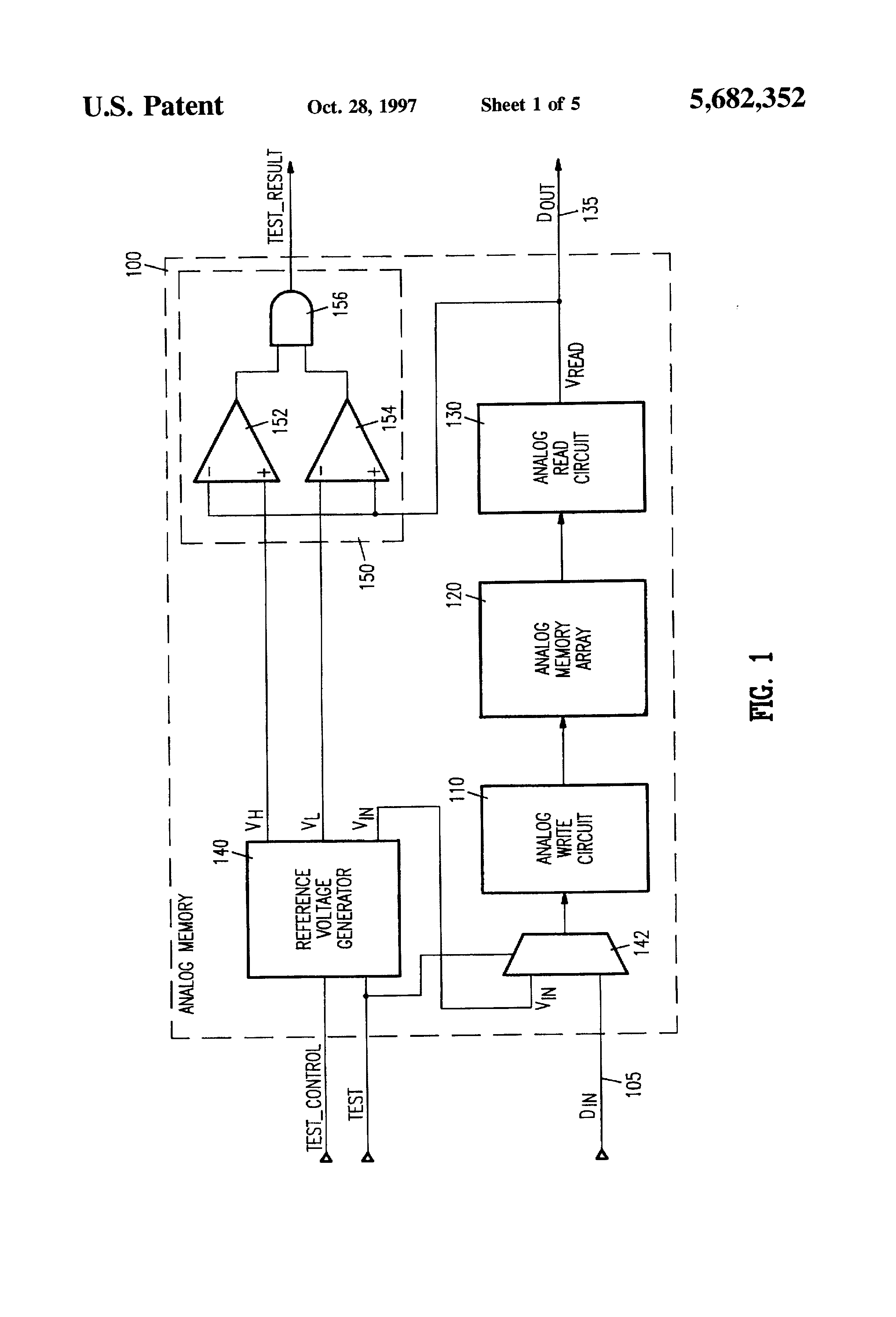
FIG. 1 shows a block diagram of an integrated analog memory 100 which is a monolithic structure and may be fabricated using conventional semiconductor IC fabrication techniques. Analog memory IC 100 contains an analog write circuit 110, an analog memory array 120, and an analog read circuit 130 which may have any design capable of writing, storing, and reading analog values. U.S. patent application No. 08/333,381, entitled "High Resolution Analog Storage EPROM and Flash EPROM", which is hereby incorporated by reference herein in its entirety, describes suitable read circuits, write circuits, and memory cells for an embodiment of the invention where channel hot electron injection is used for writing analog values to non-volatile memory cells. Another embodiment of the invention employs EEPROM or Flash EEPROM and the Fowler-Nordheim tunneling (FNT) mechanism for writing analog values. Still other embodiments of the invention can employ other types of memory not restricted to non-volatile memory. For example, analog memory array 120 could be a volatile memory such as an analog DRAM array, where each memory cell contains a capacitor and an analog value is stored as a corresponding amount of charge in a memory cell's capacitor.
During a normal write to analog memory 100, an external source such as a microphone input (not shown) asserts an analog input signal DIN which passes through a multiplexer 142 to analog write circuit 110. The voltage level of signal DIN at a particular instant represents an analog sample or value to be written to a memory cell. Typically, digital address signals are required to select cells where values are written. The address signals may be generated internally (i.e. in analog memory 100) or externally (from outside analog memory 100). Analog write circuit 110 writes a value to a selected memory cell by changing a property such as the analog memory cell's threshold voltage to a state which indicates the value written. In such embodiments, the possible threshold voltages of an analog memory cell have a one-to-one relationship with the possible voltage levels of signal DIN. The values written to analog memory array 120 remain stored as long as the analog memory cells' states are preserved.
Analog read circuit 130 reads the analog values stored in analog memory array 120. Reading generates an analog output signal DOUT having a voltage level which indicates an analog value read from analog memory array 120. For proper operation of analog memory IC 100, the value read from a memory cell should equal the value written to the memory cell. Typically, this requires that the voltage level of output data signal DOUT during reading of a value be approximately equal to the voltage level of input data signal DIN when the value was written to analog memory array 120. Some error or difference is permitted between values read and values written because exact reproduction of analog values cannot be easily achieved and is generally not required.
A range of acceptable differences between values written and values read is sometimes referred to herein as the resolution of analog memory 100 because values which differ from each other by more than the resolution can be resolved or distinguished from each other but values which differ by less than the resolution may be indistinguishable from each other after being stored. During manufacture, each analog memory IC is tested to determine its resolution. The analog memory IC can be graded according to resolution or if the resolution is very poor, discarded as defective.
To facilitate resolution determination, analog memory IC 100 contains test circuits which allow digital testing of analog functions without external analog test equipment or circuits. In particular, analog memory IC 100 contains a reference voltage generator 140 and comparison logic 150. Reference voltage generator 140 generates voltages VIN, VL, and VH which have levels selected according to a digital control signal TEST-- CONTROL. Comparison logic 150 generates a digital test result signal TEST-- RESULT based on comparisons of analog output signal DOUT to voltages VL and VH from reference voltage generator 140.
Exemplary embodiments of reference voltage generator 140 which generate voltages VIN, VL, and VH at levels dictated by digital test control signal TEST-- CONTROL are described below in regard to FIGS. 3, 4, and 5. During testing, an enable signal TEST is asserted to reference voltage generator 140 and multiplexer 142. Signal TEST is the select signal for multiplexer 142 and causes multiplexer 142 to pass voltage VIN from reference voltage generator 140 to analog write circuit 110. Analog write circuit 110 may contain an input amplifier which amplifies an input analog signal from an external source, for example, so that the maximum voltage of the input signal corresponds to the maximum value that can be written to analog memory array 120. Voltage VIN can either be input to the input amplifier or can bypass the input amplifier. When voltage VIN bypasses the input amplifier, additional testing of the input amplifier may be required. In either case, analog write circuit 110 writes a value represented by voltage VIN to a memory cell selected according to an address signal generated either internally or externally.
After writing the value represented by voltage VIN to analog memory array 120, testing proceeds with analog read circuit 130 reading the memory cell to which the value was written. Ideally, the value read is exactly equal to the value written, but a difference between the value written and the value read are acceptable if the difference is less than a resolution desired for analog memory 100. The acceptable differences between the value written and the value read prescribe a relationship between analog output signal DOUT and voltage VIN. In a typical case, the relationship which identifies a value corresponding to an input voltage also identifies a value corresponding to an output voltage, and signal DOUT must be within a fixed voltage range of voltage VIN to meet the resolution requirements. In other cases, signal DOUT is proportional to voltage VIN or related to voltage VIN in some other fashion when the value read is exactly equal to the value written, and the acceptable voltage range for signal DOUT may not contain voltage VIN.
Voltages VL and VH are the boundaries of the acceptable voltage range for analog output signal DOUT. If read circuit 130 contains an output amplifier, signal DOUT can be taken from an input terminal or an output terminal of the output amplifier provided that voltages VL and VH are properly selected. Analog output signal DOUT and voltages VL and VH are input to comparison logic 150 which determines whether signal DOUT is between voltages VL and VH. In the typical case, voltage VL is less than voltage VIN by an amount ΔV, and voltage VH is greater than VIN by ΔV, where ΔV depends on the resolution being tested. For example, if the range of analog signal DOUT is 5 volts and the desired resolution provides the equivalent of eight bits of information (256 levels), ΔV must be less than about 10 mV.
Comparison logic 150 includes analog comparators 152 and 154 and an AND gate 156. Analog comparator 152 or 154 may be a differential amplifier or op-amp which generates a digital "high" output voltage if the voltage applied to a positive input terminal of the amplifier is greater than the voltage applied to a negative input terminal of the amplifier and generates a digital "low" output voltage if the voltage applied to the positive input terminal is less than the voltage applied to the negative input terminal. Accordingly, the output voltage from analog comparator 154 is high if analog output signal DOUT is greater than voltage VL, and the output voltage from analog comparator 152 is high if analog output signal DOUT is less than voltage VH. AND gate 156 asserts signal TEST-- RESULT high if analog signal DOUT is within the range greater than voltage VL but less than voltage VH.
To measure the resolution of analog memory 100, a digital test can change digital control signals so that a gap between voltages VH and VL incrementally decreases until test result signal indicates the signal read from the memory cell is outside the range from VL to VH or incrementally increases until test result signal indicates the signal read from the memory cell is within the range from VL to VH. The difference between VL and VH as indicated by the digital control signals when the value of the result signal changes indicates the resolution of the memory cell under test.
Testing can continue by allowing analog memory 100 to sit for a period of time then re-testing the memory cells to determine if any drift in the stored values has occurred. Alternatively or additionally, the memory cells which store data are re-tested after exposing analog memory 100 to high temperatures in a bake-in process and/or after applying stress voltages to the memory cells which store data. Accordingly, the testing simulates actual use of the analog memory.
After writing a value represented by a first voltage and testing a memory cell, a second value represented by a second voltage from reference voltage generator 140 can be written to the memory cell, and the resolution of the memory cell can then be tested in the vicinity of the second value. For a more complete testing of the memory cell, values near the bottom, middle, and top of the range which can be written to memory array 100 can be tested for resolution. If memory array 100 is a non-volatile memory, writing of each value can be preceded by an erase. Alternatively, it may be possible to write successive values without erasing if the values follow an order which successively increases the threshold voltage of a memory cell.
During the above described tests, an external tester only needs to supply digital signals such as signals TEST, TEST-- CONTROL, and address signals and only needs to examine digital signals such as signal TEST-- RESULT. Accordingly, an inexpensive digital tester can test the analog read and write processes of analog memory IC 100. Additionally, the test can be more accurate than those performed by analog testers because the analog signals (i.e. intermediate voltages) generated internally for testing of analog memory IC 100 are less susceptible to noise which may arise in leads of analog testers.
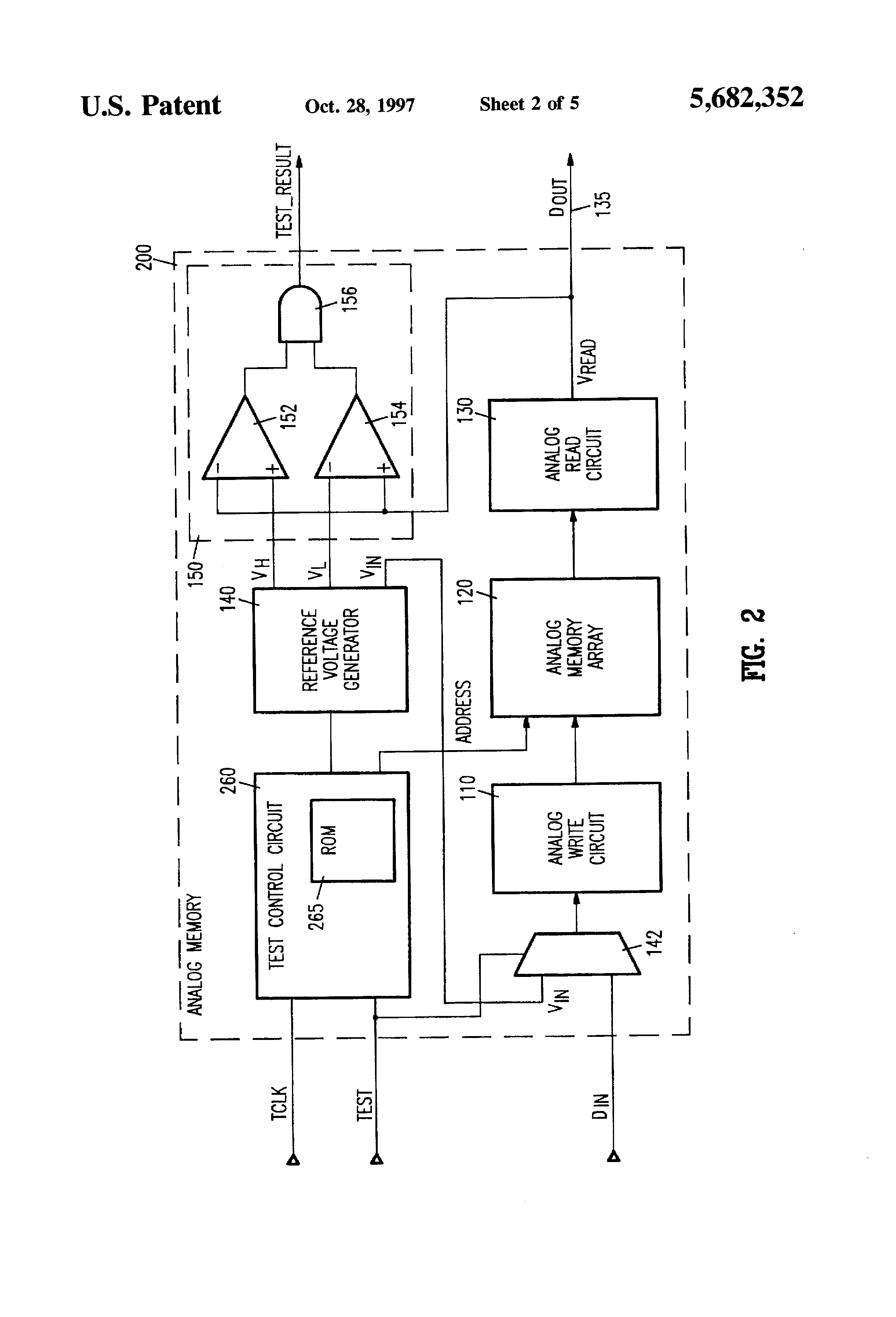
FIG. 2 shows an analog memory 200 in accordance with another embodiment of the invention. Analog memory 200 contains analog write circuit 110, analog memory array 120, analog read circuit 130, reference voltage generator 140, and comparison logic 150 such as described above in regard to FIG. 1. Analog memory 200 further includes a test control circuit 260 to reduce the number of external signals required for testing of analog memory 200. In particular, test control circuit 260, when activated by enable signal TEST, generates necessary test control signals to reference voltage generator 140 and/or address signals to analog memory array 120 as required to test the function of analog memory IC 200. Such signals may be from sequential addresses in a ROM 265. To test write and read functions of analog memory 200, an external tester asserts enable signal TEST and a clock signal TCLK to synchronize the sequence of address and control signals from test control circuit 260 with the tester. The tester then observes digital signal TEST-- RESULT to determine whether the analog functions work as desired.
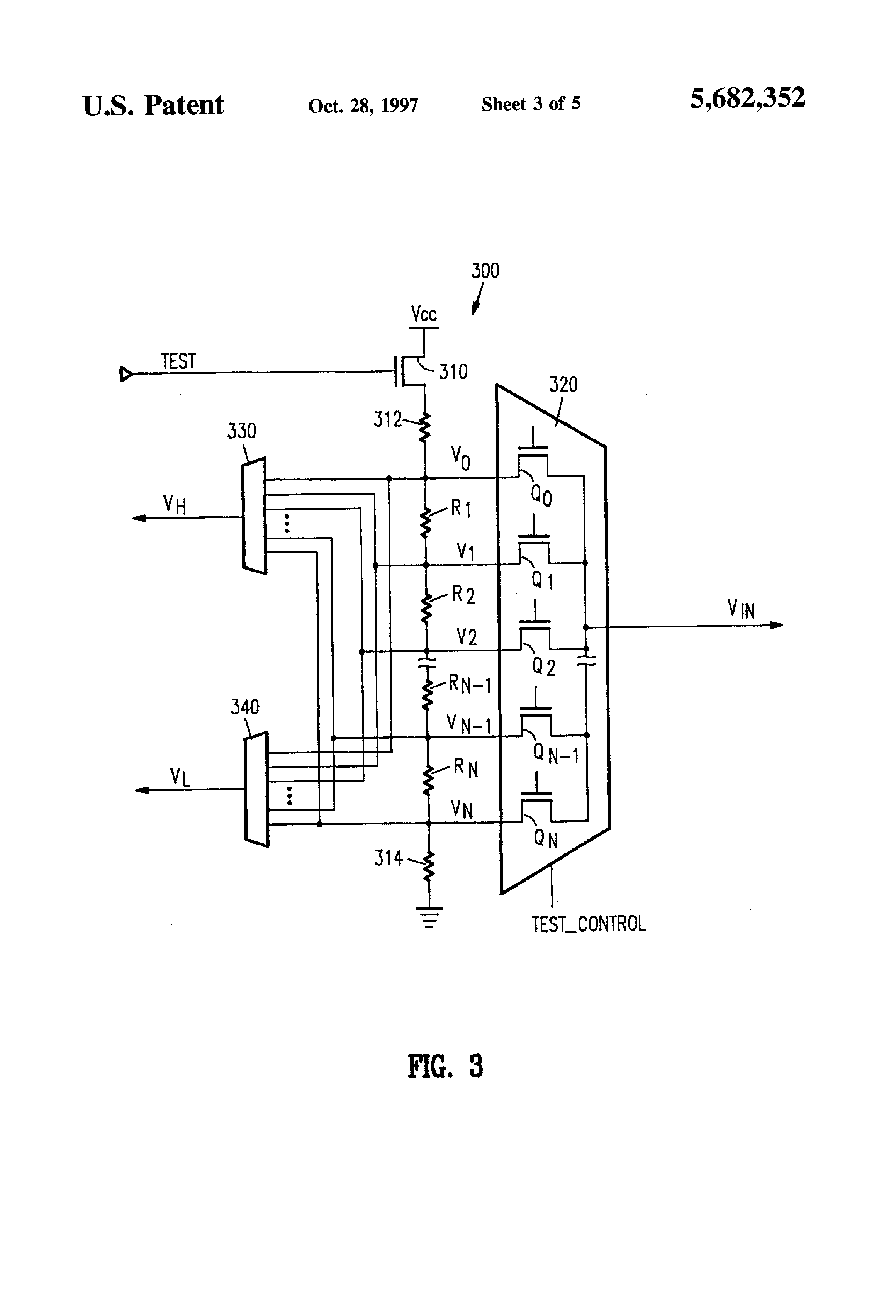
FIG. 3 shows an embodiment of a resistor tree structure 300 usable as reference voltage generator 140 in analog memory 100 (FIG. 1) or 200 (FIG. 2). Resistor tree structure 300 includes a transistor 310 and a set of resistors R1 to RN which are connected in series between a supply voltage Vcc and ground. Index N can be any desired integer. When enable signal TEST turns on a transistor 310, resistors R1 to RN act as a voltage divider, and a series of intermediate voltages V0 to VN develop at taps between resistors R1 to RN. Optionally, a resistor 312 and/or a resistor 314 can be added to the series of resistors to keep the highest intermediate voltage V0 below supply voltage Vcc and/or the lowest intermediate voltage VN above ground potential. A multiplexer 320 selects one of voltages V0 to VN as voltage VIN. Similarly, multiplexers 330 and 340 select voltages VH and VL, respectively.
In the embodiment of FIG. 3, multiplexer 320 is a collection of transistors Q0 to QN connected to taps in resistor tree structure 300, and control signal TEST-- CONTROL is a multi-bit digital signal which turns on at most one of transistors Q0 to QN to select one of voltages V0 to VN. Alternatively, any multiplexer design may be employed for multiplexers 320, 330, and 340.
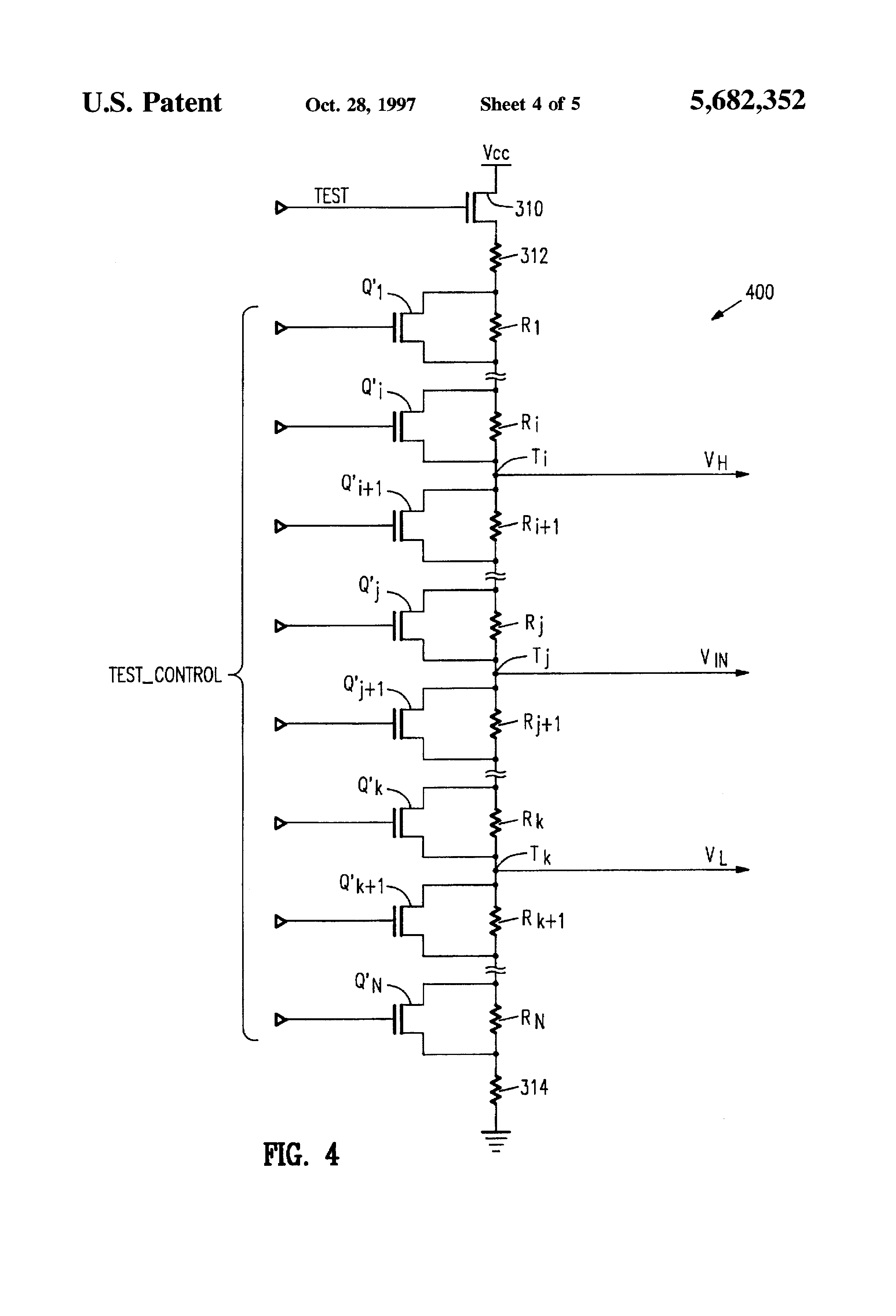
FIG. 4 shows another resistor tree structure 400 which is usable as reference voltage generator 140 in analog memory 100 or 200. Resistor tree structure 400 also contains a set of resistors R1 to RN which are connected in series; but in tree structure 400, each resistor R1 to RN is connected in parallel with a corresponding one of shunt transistors Q1 ' to QN ', and fixed taps Ti, Tj, and Tk supply voltages VH, VIN and VL. Signal TEST-- CONTROL selects levels for voltages VH, VIN and VL by turning on a desired set of shunt transistors Q1 ' to QN '. Each shunt transistor turned on creates a short across an associated resistor which increases the voltage level at taps between the transistor and ground and decreases the voltage at taps between the transistor and supply voltage Vcc. Voltage VIN is determined by the ratio of the effective resistance between tap Tj and supply voltage Vcc and the effective resistance between tap Tj and ground. Similarly, voltages VH and VL have levels determined by effective resistance above and below their respective source taps Ti and Tk.
In one embodiment of resistor tree structure 400, each of resistors R1 to RN has the same resistance. In an alternative embodiment, resistors R1 to RN have different resistances. For example, for each set of resistors such as R1 to Ri, Ri+1 to Rj, Rj+1 to Rk, and Rk+1 to RN, each resistor in the set can have twice the resistance of an adjacent resistor in the set. If the resistors in a set are related in this manner, the total resistance of the set is configurable in steps equal to the smallest resistance in the set. Alternatively, a nearly limitless number of other resistance combinations are possible.
FIG. 5 shows yet another resistor tree structure 500 which is usable as reference voltage generator 140 in analog memory 100 or 200. In tree structure 500, transistor 310 and resistors R1 to RN are connected in series between supply voltage Vcc and ground. A tap Tj, between resistors Rj and Rj+1, is the source of voltage VIN. Signal TEST-- CONTROL sets or changes voltage VIN by turning on desired ones of shunt transistors Q'1 to Q'i and Q'k+1 to Q'N which effects voltage VIN in the same manner as shunt transistors in resistor tree 400 of FIG. 4.
Multiplexer 530 selects one of taps Ti to Tj-1 as the source of voltage VH. Since taps Ti to Tj-1 are nearer supply voltage Vcc than is tap Tj, voltage VH is higher than voltage VIN. Multiplexer 540 selects one of taps Tj+1 to Tk as the source of voltage VL. Since taps Tj+1 to Tk are nearer ground than is tap Tj, voltage VL is lower than voltage VIN. If resistors Ri+1 to Rj are identical to resistors Rj+1 to Rk and the same select signals are applied to multiplexer 530 and multiplexer 540, the absolute difference ΔV between voltage VIN and VH will be equal to the absolute difference ΔV between voltage VIN and VL. Accordingly, for resistor tree 500, control signals to the shunt transistors Q'1 to Q'i and Q'k+1 to Q'N control the level of voltage VIN, and control signals to multiplexers 530 and 540 select ΔV (the resolution being tested).
Resistor trees 300, 400, and 500 are only examples of reference voltage generators in accordance with the invention. Various modification are possible. For example, separate resistor trees can provide one or more of voltages VIN, VH, and VL. Additionally, other circuits such as bandgap generators can generate required intermediate voltages, for example, when the absolute voltage levels are critical.
Although the invention has been described with reference to particular embodiments, the description is only an example of the invention's application and should not be taken as a limitation. For example, although a method for testing the resolution of an analog memory has been described, the same techniques can be used to test the accuracy of an analog output signal from any analog IC. Various other adaptations and combinations of features of the embodiments disclosed are within the scope of the present invention as defined by the following claims.