Skip to content

Patent drawings

Drawing 1 of 4

US 5,909,449

Drawing 1 of 4

Expanded drawing 1 of 4 from US 5,909,449, Multi-bit-per-cell non-volatile memory with error detection and correction
High-resolution patent drawing

US 5,909,449

Multi-bit-per-cell non-volatile memory with error detection and correction

Filed
September 8, 1997
Granted
June 1, 1999
Assignee
Sandisk
Previous Assignee
Invox
Inventors
Hock C. So, Sau C. Wong

Abstract

A multilevel non-volatile memory divides the suitable threshold voltages of memory cells into ranges corresponding to allowed states for storage of data and ranges corresponding to forbidden zones indicating a data error. A read process in accordance automatically checks whether a threshold voltage is in a forbidden zone. In alternative embodiment, a refresh process includes reprogramming the threshold voltage into an allowed state or in the case of a flash memory, reading a sector of the memory, saving data from the sector in a buffer, erasing the sector, and rewriting the data from the buffer back in the sector. Refresh process for the non-volatile memory can be perform in response to detecting a threshold voltage in a forbidden zone, as part of a power-up procedure for the memory, or periodically with a period on the order of days, weeks, or months.

View on Google Patents ↗
View Full PatentComplete archived record · 4 figures · 39 description paragraphs · 16 claims

Patent record

Source
Google Patents
Publication
US5909449A
Application
US08/924,909
Priority
September 8, 1997
Prior art date
September 8, 1997
Publication date
June 1, 1999
Legal status
Expired - Lifetime
Original assignee
Invox Technology Inc
Current assignee
SanDisk Technologies LLC
Prior art keywords
memory, threshold voltage, memory cell, data, threshold
Source retrieved
July 20, 2026

Classifications

  • GPHYSICS
  • G06COMPUTING OR CALCULATING; COUNTING
  • G06FELECTRIC DIGITAL DATA PROCESSING
  • G06F11/00Error detection; Error correction; Monitoring
  • G06F11/07Responding to the occurrence of a fault, e.g. fault tolerance
  • G06F11/08Error detection or correction by redundancy in data representation, e.g. by using checking codes
  • G06F11/10Adding special bits or symbols to the coded information, e.g. parity check, casting out 9's or 11's
  • G06F11/1008Adding special bits or symbols to the coded information, e.g. parity check, casting out 9's or 11's in individual solid state devices
  • G06F11/1072Adding special bits or symbols to the coded information, e.g. parity check, casting out 9's or 11's in individual solid state devices in multilevel memories
  • BPERFORMING OPERATIONS; TRANSPORTING
  • B64AIRCRAFT; AVIATION; COSMONAUTICS
  • B64CAEROPLANES; HELICOPTERS
  • B64C27/00Rotorcraft; Rotors peculiar thereto
  • B64C27/006Safety devices
  • G01MEASURING; TESTING
  • G01NINVESTIGATING OR ANALYSING MATERIALS BY DETERMINING THEIR CHEMICAL OR PHYSICAL PROPERTIES
  • G01N29/00Investigating or analysing materials by the use of ultrasonic, sonic or infrasonic waves; Visualisation of the interior of objects by transmitting ultrasonic or sonic waves through the object
  • G01N29/14Investigating or analysing materials by the use of ultrasonic, sonic or infrasonic waves; Visualisation of the interior of objects by transmitting ultrasonic or sonic waves through the object using acoustic emission techniques
  • G01N29/22Details, e.g. general constructional or apparatus details
  • G01N29/227Details, e.g. general constructional or apparatus details related to high pressure, tension or stress conditions
  • G06F11/1048Adding special bits or symbols to the coded information, e.g. parity check, casting out 9's or 11's in individual solid state devices using arrangements adapted for a specific error detection or correction feature
  • G06F11/106Correcting systematically all correctable errors, i.e. scrubbing
  • G11INFORMATION STORAGE
  • G11CSTATIC STORES
  • G11C11/00Digital stores characterised by the use of particular electric or magnetic storage elements; Storage elements therefor
  • G11C11/56Digital stores characterised by the use of particular electric or magnetic storage elements; Storage elements therefor using storage elements with more than two stable states represented by steps, e.g. of voltage, current, phase, frequency
  • G11C11/5621Digital stores characterised by the use of particular electric or magnetic storage elements; Storage elements therefor using storage elements with more than two stable states represented by steps, e.g. of voltage, current, phase, frequency using charge storage in a floating gate
  • G11C11/5628Programming or writing circuits; Data input circuits
  • G11C11/5635Erasing circuits
  • G11C11/5642Sensing or reading circuits; Data output circuits
  • G11C16/00Erasable programmable read-only memories
  • G11C16/02Erasable programmable read-only memories electrically programmable
  • G11C16/06Auxiliary circuits, e.g. for writing into memory
  • G11C16/10Programming or data input circuits
  • G11C16/34Determination of programming status, e.g. threshold voltage, overprogramming or underprogramming, retention
  • G11C16/3418Disturbance prevention or evaluation; Refreshing of disturbed memory data
  • G11C16/3431Circuits or methods to detect disturbed nonvolatile memory cells, e.g. which still read as programmed but with threshold less than the program verify threshold or read as erased but with threshold greater than the erase verify threshold, and to reverse the disturbance via a refreshing programming or erasing step
  • G11C16/3436Arrangements for verifying correct programming or erasure
  • G11C16/3454Arrangements for verifying correct programming or for detecting overprogrammed cells
  • G11C16/3459Circuits or methods to verify correct programming of nonvolatile memory cells
  • G11C29/00Checking stores for correct operation ; Subsequent repair; Testing stores during standby or offline operation
  • G11C29/02Detection or location of defective auxiliary circuits, e.g. defective refresh counters
  • G11C29/028Detection or location of defective auxiliary circuits, e.g. defective refresh counters with adaption or trimming of parameters
  • G11C29/04Detection or location of defective memory elements, e.g. cell constructio details, timing of test signals
  • G11C29/50Marginal testing, e.g. race, voltage or current testing
  • G11C29/50004Marginal testing, e.g. race, voltage or current testing of threshold voltage
  • G11C16/04Erasable programmable read-only memories electrically programmable using variable threshold transistors, e.g. FAMOS
  • G11C2211/00Indexing scheme relating to digital stores characterized by the use of particular electric or magnetic storage elements; Storage elements therefor
  • G11C2211/56Indexing scheme relating to G11C11/56 and sub-groups for features not covered by these groups
  • G11C2211/563Multilevel memory reading aspects
  • G11C2211/5634Reference cells

Figures

4 plates

Figure 1 of 4 from US 5,909,449, Multi-bit-per-cell non-volatile memory with error detection and correction
Figure 01Full resolution ↗
Figure 2 of 4 from US 5,909,449, Multi-bit-per-cell non-volatile memory with error detection and correction
Figure 02Full resolution ↗
Figure 3 of 4 from US 5,909,449, Multi-bit-per-cell non-volatile memory with error detection and correction
Figure 03Full resolution ↗
Figure 4 of 4 from US 5,909,449, Multi-bit-per-cell non-volatile memory with error detection and correction
Figure 04Full resolution ↗

Description

BACKGROUND

1. Field of the Invention

This invention relates to non-volatile semiconductor memory and more specifically to circuits and methods for detecting and correcting data errors in a memory storing multiple bits per memory cell.

2. Description of Related Art

Conventional electrically erasable non-volatile semiconductor memories such as E2 PROMs and flash memories have memory cells that include transistors with programmable threshold voltages. For example, a floating gate transistor or a split gate transistor has a threshold voltage that is programmed or erased by charging or discharging a floating gate located between a control gate and a channel in the transistor. The amount of charge on the floating gate of the transistor determines the voltage that must be applied to the control gate to cause charge carrier inversion in the underlying channel and therefore determines the threshold voltage of the transistor. Data is written in such memory cells by charging or discharging the floating gates of the memory cells to achieve threshold voltages corresponding to the data.

A binary memory stores one bit of data per memory cell. Accordingly, floating gate transistors in binary memory cells have two distinguishable states, a high threshold voltage state and a low threshold voltage state. Any memory cell having a threshold voltage above a cut-off threshold voltage value is in the high threshold voltage state and stores a bit value, 1 or 0, that corresponds to the high threshold state. Memory cells having threshold voltages below the cut-off are in the low threshold voltage state and store the bit value, 0 or 1, corresponding to the low threshold voltage state.

A multilevel memory stores multiple bits per memory cell. Accordingly, a range of threshold voltages for a memory cell is divided into a number of states corresponding to the possible multibit data values stored in the memory cell. For example, a memory that stores two bits of data per memory cell has a range of suitable threshold voltages for memory cells that is divided into four states. A first state includes threshold voltages below a first cut-off. A second state includes threshold voltages between the first cut-off and a second cut-off. A third state includes threshold voltages between the second cut-off and a third cut-off, and a fourth state includes threshold voltages above the third cut-off.

A concern in non-volatile semiconductor memory is drift or unintended changes in the threshold voltages of memory cells. For example, over time, charge tends to leak from the floating gates of memory cells and change the threshold voltages of the cells. Charge leakage decreases the threshold voltage of an N-channel memory cell. Alternatively, a floating gate or an insulator surrounding the floating gate can collect or trap charge and increase the threshold voltage of a cell. Further, operation of the memory, for example, programming or reading stresses memory cells not being accessed and can change threshold voltages. Changes in the threshold voltage are a problem because the state of the memory cell and the data value stored in the memory cell can change and create a data error. Such data errors are intolerable in many memory applications. The problem is worse for multilevel memories than for binary memories because the range of threshold voltages corresponding to a particular state is typically smaller in a multilevel memory which makes changes in the state of the multilevel memory cell more likely.

Multilevel memories that are resistant to data errors are sought.

SUMMARY

In accordance with the invention, a range of possible threshold voltages for a memory cell in a multilevel memory is divided into allowed states associated with data values and forbidden zones between the allowed states. A memory cell being written is programmed into an allowed state. Subsequent reading of the memory cell indicating that the threshold voltage of the memory cell is in a forbidden zone indicates that the threshold voltage of the memory cell has changed. A memory cell with a threshold voltage in a forbidden zone can be flagged as a data error or corrected by increasing or decreasing the threshold voltage to an adjacent allowed state. One specific embodiment of the invention is a flash memory that presumes charge loss in the memory cells and programs the threshold voltage of a memory cell up to the next allowed state when the memory detects that the threshold voltage of the memory cell is in a forbidden zone. Alternatively, the data error can be corrected by saving the data value in a buffer while the memory cell containing the error is erased and then programmed with the correct data value.

In accordance with another aspect of the invention, a non-volatile memory performs a refresh cycle in which memory cells are read and threshold voltages of the memory cells are reprogrammed to an allowed state. In a flash EPROM, the refresh cycle can refresh data in a single sector or an entire memory array. In alternative embodiments, the refresh cycle is triggered by external circuit attached to a monolithic integrated circuit memory or is self-triggered in the memory. Refreshes may be performed at periodic intervals of operation, as part of a power-up procedure for the memory, or transparently during each read operation performed by the memory.

According to a further aspect of the invention, adjacent states (i.e., ranges of threshold voltages) for a multilevel memory cell are mapped to data values using gray coding or another coding system instead of a direct monotonic mapping from threshold voltages to data values. With such coding, a drift from one threshold voltage state to an adjacent threshold voltage state causes only a single bit error. Such single bit errors can be detected and corrected using error correction codes. The gray coding of allowed states can be used with or without forbidden zones between the coded states and/or refresh cycles to correct stored data.

BRIEF DESCRIPTION OF THE DRAWINGS

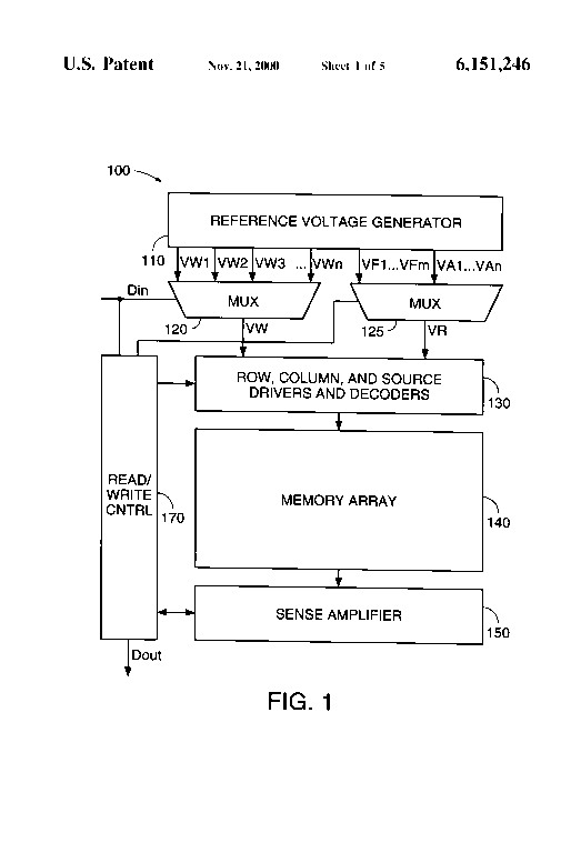
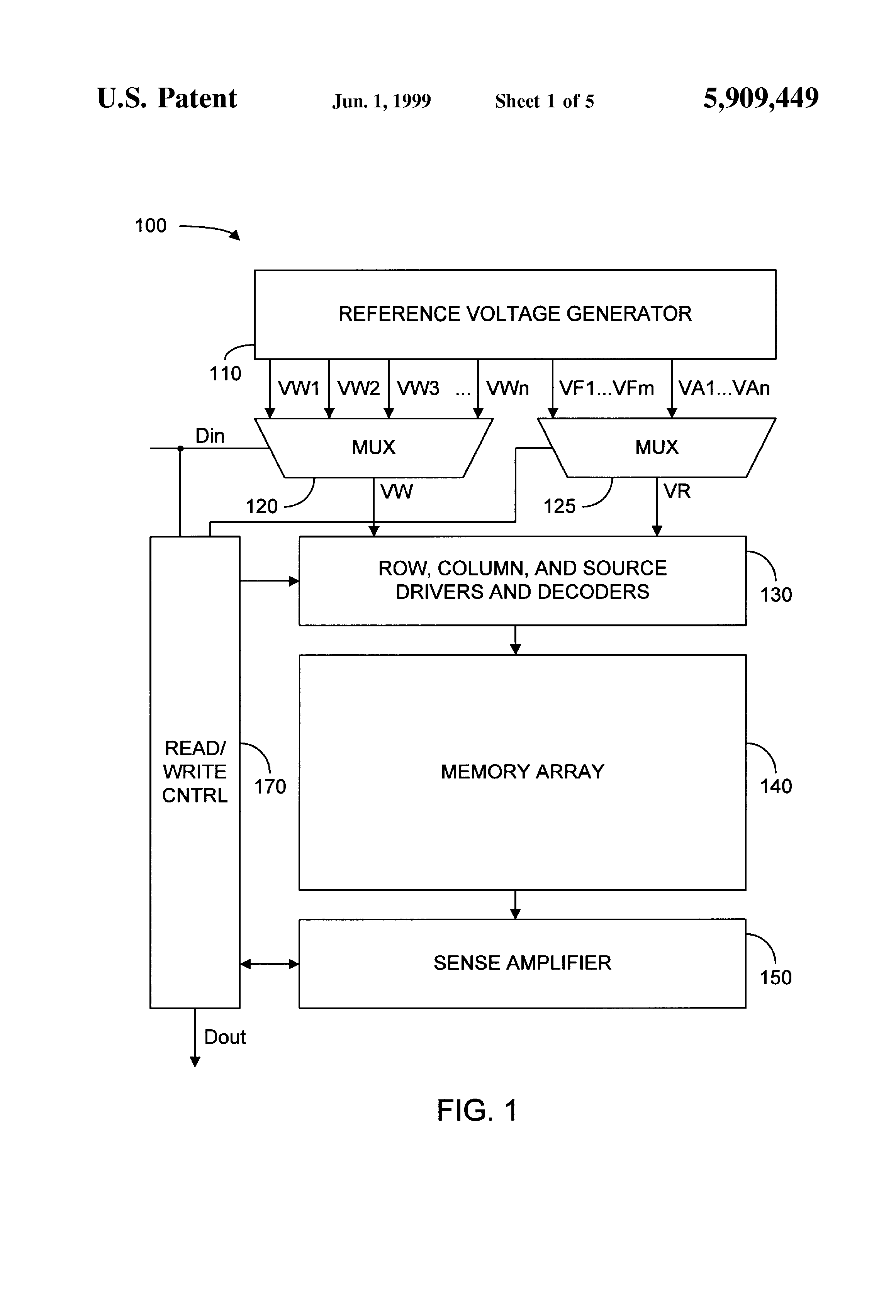
FIG. 1 shows a block diagram of a multilevel memory in accordance with an embodiment of the invention.

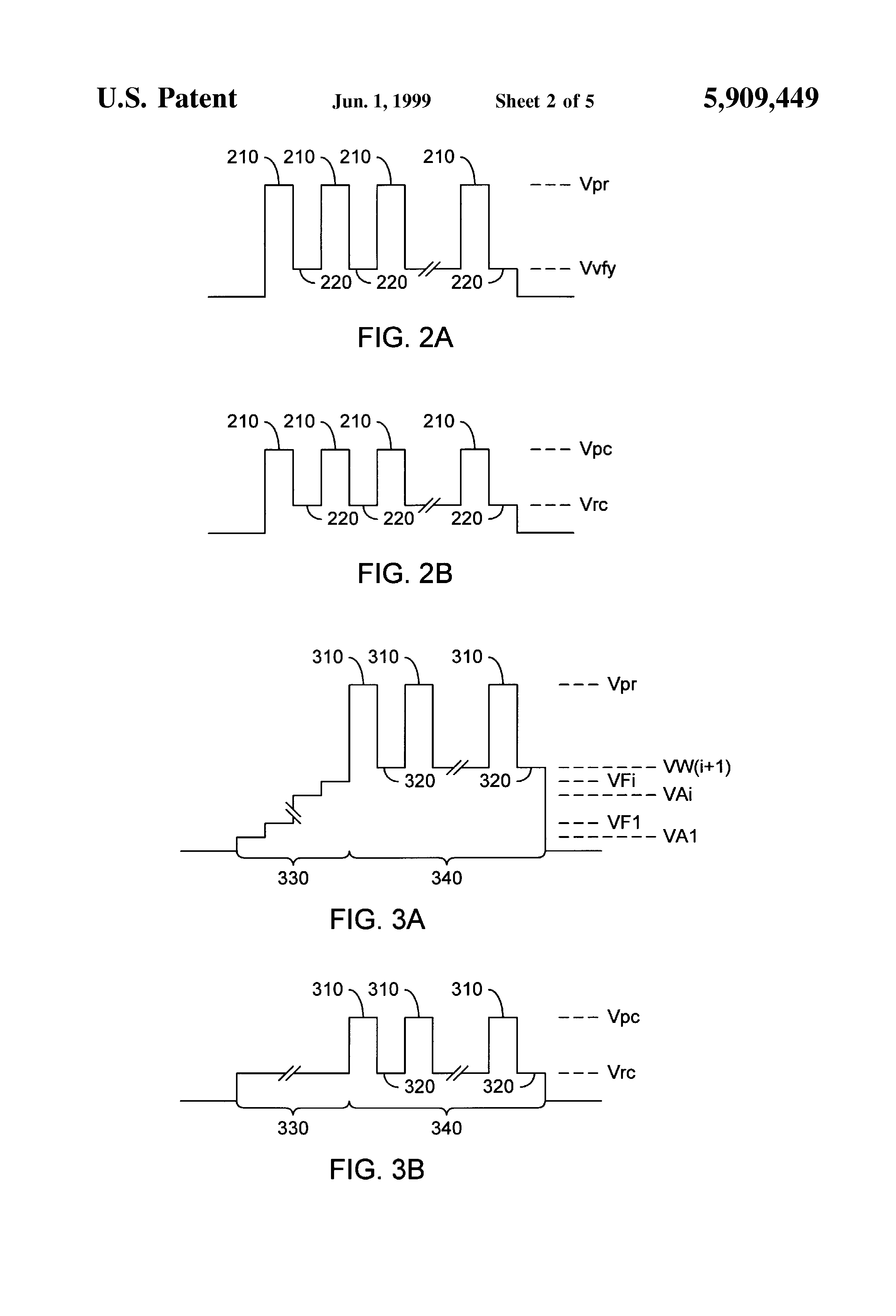
FIGS. 2A and 2B respectively show a row line voltage and a column line voltage during a write operation in the memory of FIG. 1.

FIGS. 3A and 3B respectively show a row line voltage and a column line voltage during a read/refresh operation in the memory of FIG. 1.

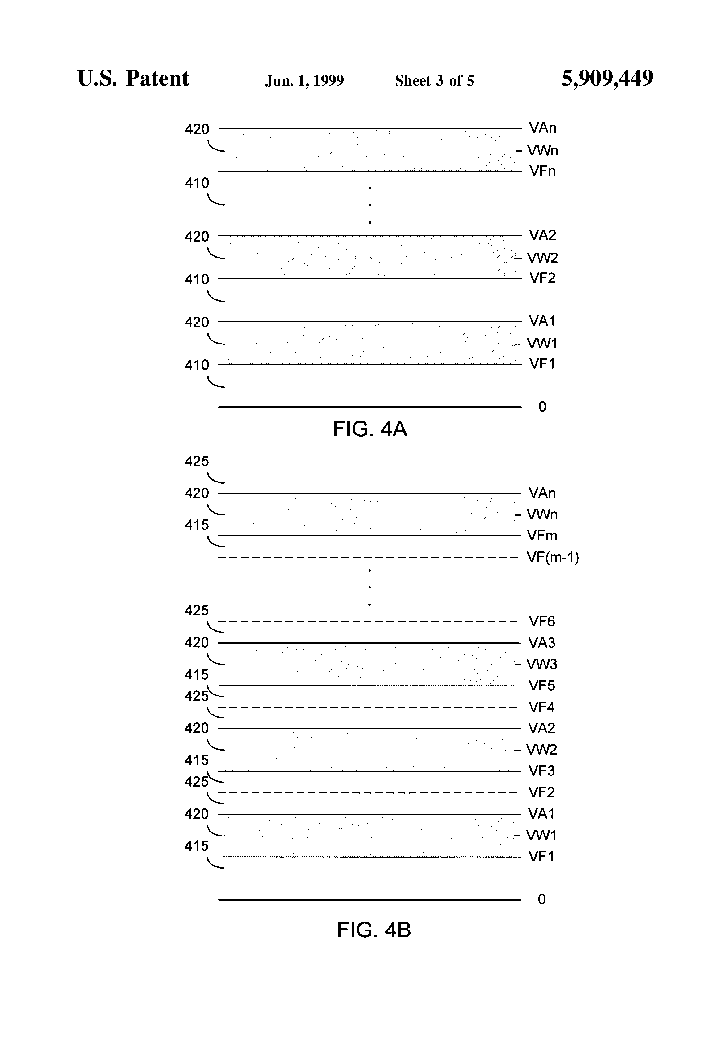
FIGS. 4A and 4B show partitions of threshold voltage ranges into allowed states and forbidden zones in accordance with an embodiment of the invention.

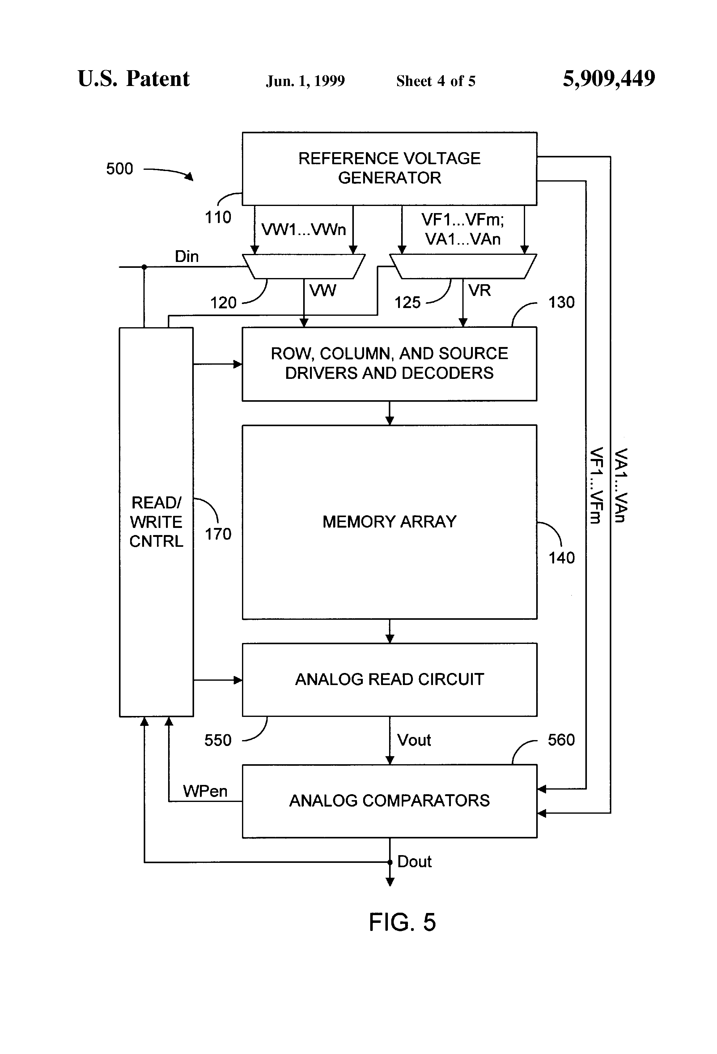
FIG. 5 shows a block diagram of a multilevel memory in accordance with another embodiment of the invention.

FIG. 6 shows a block diagram of a multilevel non-volatile memory system with refresh circuits in accordance with an embodiment of the invention.

Use of the same reference symbols in different figures indicates similar or identical items.

DETAILED DESCRIPTION OF THE PREFERRED EMBODIMENTS

A multilevel memory in accordance with an embodiment of the invention partitions a range of threshold voltages of a memory cell into a set of allowed states that correspond to data values that can be stored in the memory cell and a set of forbidden zones. The allowed states are separated from each other by forbidden zones so that if the threshold voltage of a memory cell drifts it must cross through a forbidden zone before reaching another allowed state. A memory cell detected as having a threshold voltage in one of the forbidden zones indicates a data error which can be automatically corrected during a read or reported as an error for subsequent correction and refresh procedure. FIG. 1 illustrates a multilevel memory 100 in accordance with an embodiment of the invention. Memory 100 includes a memory array 140. In an exemplary embodiment of the invention, memory 100 is a flash EPROM, and array 140 includes hundreds or thousands of rows or columns of N-channel floating gate transistors (memory cells) organized into independently erasable sectors. Each row of memory cells has control gates coupled to a row line for the row, and each column of memory cells has drains coupled to a column line for the column. Each erasable sector has a source line coupled to the sources of memory cells in the sector. Row, column, and source drivers and decoders 130 are coupled to memory array 140 and generate voltages that are applied to selected row, column, and source lines in memory array 140 for erase, write, and read operations. For an erase, drivers and decoders 130 apply appropriate voltages to the memory cells in a sector to cause Fowler-Nordheim tunneling that removes electrons from the floating gates and reduces the threshold voltage of the memory cells in the sector. For a write operation, drivers and decoders 130 apply programming voltages to the row, column, and source lines coupled to a target memory cell to cause channel hot electron injection that increases the threshold voltage of the target memory cell to a level indicating a data value being written. As will be understood, applications of the invention are not limited to flash EPROM of the exemplary embodiment but can be employed in a variety of memory architectures including but not limited to EPROM, E2 PROM, and flash E2 PROM.

A read/write control circuit 170 controls writing to a target memory cell in memory array 140. For a write, an input digital data signal Din representing a multibit value to be written to the target memory cell is a select signal for a multiplexer 120. Signal Din is restricted to the number of bits that can be written to a single memory cell. Data values containing more bits than can be stored in a single memory cell may be split into parts containing the number of bits, e.g., 2, 3, 4 . . . bits, that can be stored in a single memory cell so that the parts can be written sequentially to memory cells using the circuitry shown in FIG. 1 or in parallel using parallel circuits (not shown.) Multiplexer 120, which is coupled to a reference voltage generator 110, selects one of input reference signals VWl to VWn, where n is the number of possible data values that can be stored in a memory cell. (For example, n is sixteen (2x) for memory storing 4-bits (x-bits) per memory cell.) Multiplexer 120 generates an analog signal VW to drivers and decoders 130 to indicate the value being written.

The write process proceeds as illustrated in FIGS. 2A and 2B. In particular, during a series of programming cycles 210, drivers and decoders 130 generate and apply programming voltages Vpr and Vpc to the row and column lines of a target memory cell while grounding the source line of the sector containing the target cell. In the exemplary embodiment, programming voltage Vpr is between 7 and 11 volts and depends on signal VW. Drivers and decoders 130 may include, for example, a row line driver containing voltage shifter or amplifier having signal VW as an input signal and voltage Vpr as an output signal. Alternatively, voltage Vpr may be a fixed voltage, independent of signal Vin. A conventional row decoder applies voltage Vpr to the row line coupled to the target memory cell. A conventional column decoder applies voltage Vpc to the drain of the target memory cell during programming cycles 210. Voltage Vpc is typically about 6 volts or whatever voltage is required to increase the threshold voltage of the target memory cell by channel hot electron (CHE) injection of electrons into the floating gate of the target memory cell. Alternative embodiments of the invention using, for example, E2 PROM technology program memory cells by tunneling instead of CHE injection.

Verify cycles 220 are performed between programming cycles 210 to determine whether the threshold voltage of the target memory cell has reached the desired level. During each verify cycle, drivers and decoders 130 apply to the control gate of the target memory cell a voltage Vvfy which depends on (or is equal to) voltage VW (i.e., one of reference voltages VWl to VWn), grounds the source lines, and applies a read voltage Vrc to the column line of the target memory cell. A sense amplifier 150 senses whether the target memory cell conducts. If the target memory cell conducts during a verify cycle 220, the threshold voltage of the memory cell is less than voltage Vvfy, and read/write control 170 starts another programming cycle 210 to further increase the threshold voltage. If the target memory cell does not conduct during a verify cycle 220, the threshold voltage has exceeded (but is about equal to voltage Vvfy), and read write control 170 stops further programming cycles 220.

Read/write control 170 also controls read and refresh processes in accordance with an embodiment of the invention. FIGS. 3A and 3B respectively show a row line voltage and a column line voltage during an exemplary combined read/refresh process performed on a target memory cell. During a read stage 330 of the read/refresh process, drivers and decoders 130 ground the source lines, apply a constant read voltage Vrc (typically about 1 to 2 volts) to the column line coupled to the target memory cell, and apply a series of reference voltages from reference voltage generator 110 to the row line (and therefore the control gate) of the target memory cell. For each reference voltage applied to the row line during read stage 330, sense amplifiers 150 sense whether the target memory cell conducts. The applied reference voltages during read stage 130 indicate the bounds of allowed threshold voltage states and of forbidden threshold voltage zones such as illustrated in FIG. 4A. In FIG. 4A, reference voltages VFl to VFm mark the upper bounds of forbidden zones 410 and the lower bounds of allowed threshold voltage states 420. Reference voltages VAl to VAn mark the upper bounds of allowed threshold states 420 and the lower bounds of forbidden zones 410. Each of the reference voltage levels VW1 to VWn are within an associated one of allowed states 420 so that a write operation ends with a threshold voltage of a target memory cell being in the allowed state 420 associated with the reference voltage VW. To provide the desired reference voltages as shown in FIG. 4A (or 4B), reference voltage generator 110 may contain a voltage source coupled to series connected resistive elements with taps between the resistive elements for the reference voltages VWl to VWn, VFl to VFm, and VAl and VAn.

During read stage 330, read/write control 170 uses multiplexer 125 to select reference voltages applied to through drivers and decoders 130 to the row line coupled to the target memory cell. Reference voltages starting with lowest reference voltage (voltage VFl in FIG. 4A) are sequentially applied in order of increasing voltage until sense amplifier 150 senses that applied voltage VR causes the target memory cell to conduct. Thus, at the end of read stage 330, voltage VR is upper bound of the allowed state or forbidden zone containing the threshold voltage of the target memory cell. An alternative read process to that shown in FIGS. 3A and 3B starts at the maximum reference voltage VAn and proceeds in order of decreasing threshold voltage to find a lower bound of the allowed state or forbidden zone containing the threshold voltage of the target memory cell. Yet another read process starts at a reference voltage in the middle of the range of reference voltages and identifies which half (upper or lower) of the range contains the target threshold voltage. (If the memory cell conducts when the middle reference value is applied, the threshold voltage of the target memory cell is in the lower half. Otherwise, the threshold voltage of the target memory cell is in the upper half.) Second and if necessary third and subsequent reference voltages applied to the control gate are in the middle of the range previously identified as containing the threshold voltage of the target memory cell. Sensing for these threshold voltages identifies which quarter, eighth, or smaller division of the threshold voltage range contains the threshold voltage of the target cell. When the division identified is a single allowed state or forbidden zone, the reference voltage that is just above the threshold voltage of the target memory cell is identified. An advantage of the last read process is an on-average decrease in the number of reference voltages applied and sensed from 2x-1 to x where x is the number of bits stored per memory cell. Thus, the last read process provides better average performance for memory storing more than two bits per memory cell.

Voltage VR at the end of read stage 330 indicates the upper bound of either an allowed state or a forbidden zone containing the threshold voltage of the target memory cell. Read/write control 170 generates a multibit digital data signal Dout based on the bound that voltage VR identifies. If voltage VR at the end of read stage 330 is an upper bound of an allowed state, signal Dout indicates the multibit value associated with that state. If voltage VR is an upper bound of a forbidden zone, value Dout indicates the multibit value associated with the allowed state just above the forbidden zone containing the threshold voltage of the memory cell. Thus, this read process assumes that the threshold voltage of the target memory drifted down which is the most common type of change in threshold voltage for N-channel floating gate transistors. If voltage VR is the upper bound of an allowed threshold voltage state at the end of read stage 330, the read/refresh process is complete. No refresh is required. However, if as in FIGS. 3A, voltage VR is the upper bound of a forbidden zone, a refresh stage 340 of the read/refresh process begins.

During refresh stage 340, programming cycles 310 and verify cycles 320 raise the threshold voltage of the target memory cell to the next higher threshold voltage state. In the particular example of FIGS. 3A and 3B, voltage VR is equal to reference voltage VFl at the end of read stage 330, and signal Dout identifies the multibit value corresponding to the next greater allowed level and to reference voltage VW(i+1). Read/write control 170 feeds signal Dout back to multiplexer 120 which sets voltage VW equal to the reference voltage VW(i+1). Thus, during programming cycles 310 and verify cycles 320, programming voltage Vpr and verify voltage Vvfy are appropriate for the value being refreshed. As in the write process described above, programming cycles 310 continue until a verify cycle 320 indicates that the threshold voltage of the target cell has reached the level of reference voltage VW(i+1) after which refresh stage 340 is complete.

FIG. 5 shows an alternative multilevel non-volatile memory 500 in accordance with an embodiment of the invention. Memory 500 differs from memory 100 of FIG. 1 primarily in that a read uses an analog read circuit 550 and comparators 560, not sense amplifiers 150. In particular, instead of repeatedly sensing whether the target memory cell conducts when a series of different reference voltages is applied to the control gate of the memory cell, analog read circuit 550 generates an analog voltage Vout that indicates the threshold voltage of the target memory cell. In an alternative embodiment, analog read circuit generates a signal having a current that indicates the threshold voltage of a target memory cell. U.S. patent application Ser. No. 08/585,072, entitled "Read Circuits for Analog Memory Cells"; U.S. patent application Ser. No. 08/622,333, entitled "Feedback Loop for Threshold Voltage Measurement"; and U.S. patent application Ser. No. 08/622,332, entitled "Read Circuit that uses a Coarse-to-Fine Search when Reading the Threshold Voltage of a Memory Cell" describe suitable analog read circuits and are incorporated by reference herein in their entirety. Analog comparators 560 operate in parallel to compare voltage Vout to reference voltages VAl . . . VAn and VFl . . . VFN. From the results of the comparisons, logic (not shown) coupled to analog comparators 150 determines which is the smallest reference voltage greater than voltage Vout and generates digital output signal Dout. The architecture of memory 500 typically provides faster reads than memory 100 if generating signal Vout is faster than applying as series of reference voltages.

Alternatively, analog comparators 560 include one comparator or fewer comparators than there are references voltages VAl . . . VAn and VFl . . . VFN, and the comparator or comparators sequentially compare voltage Vout to each references voltages VAI . . . VAn and VFl . . . VFN. Any sequence of comparisons can be made. For example, comparisons searching for the nearest reference voltage can start from a highest, lowest, or middle reference voltage and proceed until the range containing Vout is found. This embodiment of the invention can decrease circuit size and cost but increases the read time.

The write/refresh process described above assumes that a threshold voltage in a forbidden zone indicates a memory cell that leaked charge which decreased the threshold voltage of the memory cell. However, threshold voltages can also increase as the result of charge trapping in a floating gate or in the insulator surrounding the floating gate. FIG. 4B illustrates reference voltage levels VFl to VFm that define two forbidden zones 415 and 425 between each adjacent pair of allowed states 420. Each forbidden zone 415 is just below an adjacent allowed state 420. Each forbidden zone 425 is just above an adjacent allowed state 420. In accordance with this embodiment of the invention, a data error that occurs when a memory cell has a threshold voltage in one of forbidden zones 415 is presumed to result from charge loss from a memory cell originally in the adjacent higher allowed state 420. Thus, read/write control 170 decodes a threshold voltage in a forbidden zone 415 as data values corresponding to the next higher allowed state 420. A threshold voltage in one of forbidden zones 425 is presumed to result from charge trapping or another mechanism increasing the threshold voltage from the adjacent lower allowed state 420. Read/write control 170 decodes a threshold voltage in a forbidden zone 425 as data values corresponding to the next lower allowed state 420.

Threshold voltages in forbidden zones 415 can be corrected by programming the memory cell up to the next allowed state. Similarly, if a memory architecture provides a method for individual erasing or reducing the threshold voltage of a single memory cell, a threshold voltage in a forbidden zone 425 can be lowered to the next lower allowed state. However, a typical flash memory architecture erases sectors as a unit and does not provide a mechanism for erasing or reducing the threshold voltage of individual memory cells. In such flash architectures, a sector containing a data error can be marked as requiring a refresh. Special memory cells in the array or a separate register can be used to identify the data sectors marked for a refresh. FIG. 6 illustrates a system 600 capable of performing scheduled or delayed refreshes of sectors. In system 600, a read detecting a data error caused when a memory cell is in a forbidden zone signals a refresh control 620 that can be an on-chip component integrated with memory 100 or an off-chip component. The refresh for a data sector marked as containing a data error need not be immediate. Instead refresh control 620 can wait for a period of inactivity of memory 100 before initiating a refresh of the marked sector.

To perform a refresh of an erasable sector, refresh controller 620 reads data from the sector and temporarily stores the data in a buffer 610 while the data sector is erased. Buffer 610 can be on-chip or off-chip volatile memory such as SRAM or DRAM or non-volatile memory. Refresh control 620 rewrites data from buffer 610 to the sector after the erase. During the refresh of a data sector, refresh control 620 can perform arbitration to avoid accessing of a sector being erased. For example, memory 100 may be flagged as temporarily unavailable; or alternatively, refresh control 620 can reroute an access, particularly a read, to buffer 610.

System 600 also includes a timer 630 for systematic memory refreshes and delaying flagged refreshes until a convenient time. In alternative embodiments of the invention, timer 630 is on-chip or is an off-chip component. As described above, a typical refreshes affects a sector but an entire memory can be refreshed sector by sector if desired. Such refreshes can keep data accurately stored in nonvolatile memory for extended periods of time even if the data is not otherwise read periodically. In one embodiment of the invention, memory refreshes are periodic with a period shorter than the time required for a non-defective memory cell to drift from one allowed state, across a forbidden zone to another allowed state or a forbidden zone corresponding to another allowed state. Such periods are typically be on the order of weeks or months for current non-volatile memory but more frequent refreshes having a period of on the order of a day or less can be used. Because of the long intervals between refreshes, periodic memory refreshes may be scheduled for times when use of the memory is less likely. Selection of the time for a refresh can be selected according to the time of the day or the day of the week to select a time when memory access is unlikely, for example, midnight on a Sunday. Refresh control 620 can also monitor memory access to select and further delay a refresh until detecting a suitably long period of memory inactivity. The last date and time of a refresh can be stored on-chip and checked periodically when the memory is powered. Additionally or alternatively, refresh control 620 can conduct a full or partial refresh of memory 100 as part of a power-up procedure for memory 100.

As another aspect of the invention, a mapping between allowed threshold voltage states and digital values maps adjacent threshold voltage levels to multibit values that differs only in a single bit. Accordingly, the threshold voltage of a memory cell drifting from one threshold voltage state to an adjacent state causes a single bit error. In contrast, for conventional data coding, which monotonically maps threshold voltages states with increasing (or decreasing) threshold voltage to sequentially increasing binary values, a memory cells threshold voltage drifting a single state can cause a multibit error.

Table 1 illustrates two data coding schemes for a multilevel memory that stores one 4-bit value per memory cell. To store a 4-bit value in a memory cell, sixteen allowed states are allocated in the range of possible (or suitable) threshold voltages for the memory cell. For Table 1, a threshold voltage ranging between 1 and 5 volts is partitioned into sixteen allowed states designated levels 1 to 16.

The linear coding according of Table 1 maps threshold voltage levels 1 to 16 in order of increasing threshold voltage to sequentially increasing binary values 0000 to 1111. With linear coding, if the threshold voltage of a memory cell is programmed to threshold voltage level 9 but drifts down to threshold voltage level 8, a 4-bit error occurs. In contrast, for the gray coding of Table 1, a threshold voltage drifting to an adjacent allowed state causes only a single bit error.

As a further aspect of the invention, error correction codes can be generated and stored for a section, row, column, or other part of a memory and used to correct data errors. In particular, when a threshold voltage is observed in a forbidden zone, an error correction code generated when data was written can be used to determine the correct allowed threshold voltage state for a memory cell. The error correction codes can identify the correct threshold voltage states when reading or refreshing memory cells. The gray coding of Table 1 is well suited to use with error correction codes since single bit errors are typically easier to correct with error correction codes than are multiple bit errors.

The gray coding process of Table 1 can be varied in a variety of ways. For example, many different mappings which provide a series of values where adjacent values differ by a single bit are possible. Such mappings are not restricted to 4-bit data values but are known for any size of multibit data values. Also, although Table 1, describes allowed states which are separated from each other to provide forbidden zones between the allowed states, gray coding of multibit values in a memory cell is applicable to memories where the range of threshold voltages for a memory cell does not includes forbidden zones between the allowed states.

To implement the gray coding of Table 1 in memory array 100, multiplexer 120 implements the mapping between a 4-bit digital value Din as in column 4 of Table 1 to a voltage VW that is within a voltage range indicated in column 2 of Table 1. Read/write control 170 performs the reverse mapping from VR at the end of the read stage the associate digital value in column 4 of Table 1.

Although the invention has been described with reference to particular embodiments, the description is only an example of the inventions application and should not be taken as a limitation. In particular, even though much of preceding discussion was aimed at non-volatile memory including N-channel floating gate devices, alternative embodiments of this invention include other memory structures. For example, embodiments employing P-channel transistors are possible. In such embodiments, erasing and charge leakage increase the threshold voltage of a memory cell, and programming decreases the threshold voltages. Accordingly, variations in the read and write processes described above are required. Various other adaptations and combinations of features of the embodiments disclosed are within the scope of the invention as defined by the following claims.
Claims (16)

  1. A non-volatile semiconductor memory comprising: an array of memory cells; drivers and decoders coupled to apply voltages to the array, as required to write to any memory cell in the array and to read any memory cell in the array, wherein each memory cell that stores data has a threshold voltage that identifies a multibit data value written in the memory cell; a reference generator that generates first reference signals and second reference signals, wherein the first reference signals indicate bounds of ranges of threshold voltages allowed for the memory cells storing data, and the second reference signals indicate bounds of one or more ranges of threshold voltages forbidden for the memory cells storing data; and a control circuit coupled to control the drivers and decoders during a read process, the control circuit including logic that initiates a process to refresh a threshold voltage of a memory cell during a read process that detects the threshold voltage of the memory cell is in a range forbidden for memory cells storing data.
  2. The non-volatile memory of claim 1, further comprising a timer that triggers a refresh operation by initiating reading of at least a portion of the memory array.
  3. The non-volatile memory of claim 2, wherein the array, the drivers and decoders, the reference generator, the control circuit, the timer are parts of a monolithic integrated circuit.
  4. The non-volatile memory of claim 2, further comprising a buffer coupled to temporarily store data from the portion of the memory array, during the refresh operation.
  5. The non-volatile memory of claim 1, wherein the ranges of threshold voltages allowed for memory cells storing data are separated from each other by at least one range of threshold voltages forbidden for memory cells storing data.
  6. A method for operating a non-volatile memory, comprising: measuring a threshold voltage of a memory cell; generating a multibit digital signal corresponding to the threshold voltage; identifying whether the threshold voltage is in one of a first plurality of ranges of threshold voltages or in one of a second plurality of ranges of threshold voltages; and in response to the threshold voltage being in one of the first plurality of ranges of threshold voltages, changing the threshold voltage so that the threshold voltage is in one of the second plurality of ranges of threshold voltages.
  7. The method of claim 6, wherein changing the threshold voltage changes the threshold voltage so that the threshold voltage is in a range that corresponds to the multibit digital signal.
  8. The method of claim 6, wherein: the second plurality of ranges of threshold voltages form a sequence of ranges ordered according to increasing maximum voltages of the ranges; each range corresponds to a different multibit digital value; and the multibit digital value for each range differs by only one bit, from the multibit value for the range immediately preceding in the series.
  9. The method of claim 6, wherein the steps of claim 6 are performed as part of a standard read operation for the memory.
  10. A method for operating a non-volatile memory, comprising: programming threshold voltages of memory cells in the non-volatile memory so that each memory cell has a threshold voltage in an allowed state associated with a multibit data value stored in the memory cell, wherein threshold voltages of the memory cells have a plurality of allowed states that are separated from each other by forbidden zones; identifying a portion of the non-volatile memory that contains a memory cell with a threshold voltage in one of the forbidden zones; and refreshing the multibit data values stored in memory cells in the identified portion by reprogramming the threshold voltages.
  11. The method of claim 10, wherein refreshing the multibit data values is performed in response to a signal from a timer.
  12. The method of claim 11, wherein refreshing the multibit data values is performed periodically with a period greater than one day.
  13. The method of claim 11, further comprising determining a time during which use of the memory is unlikely, wherein the timer schedules refreshing for that time.
  14. The method of claim 10, wherein refreshing the multibit data values is performed as part of a power up procedure for the memory.
  15. The method of claim 10, wherein the portion identified as containing a memory cell with a threshold voltage in one of the forbidden zones is a sector, and refreshing the multibit data values comprises: reading data values from the sector; storing the data values in a buffer; erasing the sector; and writing the data values back in the sector.
  16. The method of claim 10, wherein reading the data values comprises measuring the threshold voltage of the memory cell with the threshold voltage in one of the forbidden zones, wherein a data value read from that memory cell corresponds to an allowed state near the forbidden zone containing the threshold voltage of the memory cell.

Publications

Related applications (15)

  1. US08/924,909

    Priority application

  2. JP25206498A

    Priority application

  3. EP98307184A

    Priority application

  4. US09/200,220

    Priority application

  5. US09/680,797

    Priority application

  6. US10/045,505

    Priority application

  7. US11/101,938

    Priority application

  8. US11/620,127

    Priority application

  9. US08/924,909

    Claims priority

  10. US08/924,909

    Patent family

  11. US09/200,220

    Patent family

  12. US09/680,797

    Patent family

  13. US10/045,505

    Patent family

  14. US11/101,938

    Patent family

  15. US11/620,127

    Patent family

Record timeline

  1. Priority to US08/924,909

  2. Assigned to INVOX TECHNOLOGY

  3. Application filed by Invox Technology Inc

  4. Priority to JP25206498A

  5. Priority to EP98307184A

  6. Priority to US09/200,220

  7. Publication of US5909449A

  8. Application granted

  9. Priority to US09/680,797

  10. Assigned to SANDISK CORPORATION

  11. Priority to US10/045,505

  12. Priority to US11/101,938

  13. Priority to US11/620,127

  14. Assigned to SANDISK TECHNOLOGIES INC.

  15. Anticipated expiration

  16. Expired - LifetimeCurrent

Legal events

  1. AS

    Assignment

    Owner name: INVOX TECHNOLOGY, CALIFORNIA

    Free format text: ASSIGNMENT OF ASSIGNORS INTEREST;ASSIGNORS:SO, HOCK C.;WONG, SAU C.;REEL/FRAME:008705/0143

    Effective date: 19970908

  2. STCF

    Information on status: patent grant

    Free format text: PATENTED CASE

  3. AS

    Assignment

    Owner name: SANDISK CORPORATION, CALIFORNIA

    Free format text: ASSIGNMENT OF ASSIGNORS INTEREST;ASSIGNOR:INVOX TECHNOLOGY;REEL/FRAME:011812/0888

    Effective date: 19990920

  4. FEPP

    Fee payment procedure

    Free format text: PAT HOLDER NO LONGER CLAIMS SMALL ENTITY STATUS, ENTITY STATUS SET TO UNDISCOUNTED (ORIGINAL EVENT CODE: STOL); ENTITY STATUS OF PATENT OWNER: LARGE ENTITY

  5. REMI

    Maintenance fee reminder mailed

  6. FPAY

    Fee payment

    Year of fee payment: 4

  7. SULP

    Surcharge for late payment

  8. FPAY

    Fee payment

    Year of fee payment: 8

  9. FPAY

    Fee payment

    Year of fee payment: 12

  10. AS

    Assignment

    Owner name: SANDISK TECHNOLOGIES INC., TEXAS

    Free format text: ASSIGNMENT OF ASSIGNORS INTEREST;ASSIGNOR:SANDISK CORPORATION;REEL/FRAME:026223/0838

    Effective date: 20110404

Patent citations (3)

  1. US4964079A

    Electrically programmable memory with several information bits per cell

    Sgs-Thomson Microelectronics · October 16, 1990 · Examiner cited

  2. US5689465A

    Semiconductor memory device and defective memory cell correction circuit

    Texas Instruments Incorporated · November 18, 1997 · Examiner cited

  3. US5751639A

    DRAM having a power supply voltage lowering circuit

    Kabushiki Kaisha Toshiba · May 12, 1998 · Examiner cited

Cited by (323)

  1. US20080219049A1

    Electrically alterable non-volatile memory with n-bits per cell

    Banks Gerald J · September 11, 2008 · Examiner cited

  2. US20100020616A1

    Soft Errors Handling in EEPROM Devices

    Auclair Daniel L · January 28, 2010 · Examiner cited

  3. US7616484B2

    Soft errors handling in EEPROM devices

    Sandisk Corporation · November 10, 2009

  4. US7839685B2

    Soft errors handling in EEPROM devices

    Sandisk Corporation · November 23, 2010

  5. US20050083726A1

    Soft errors handling EEPROM devices

    Auclair Daniel L. · April 21, 2005 · Examiner cited

  6. US20050058008A1

    Soft errors handling in eeprom devices

    Auclair Daniel L. · March 17, 2005 · Examiner cited

  7. US20040237010A1

    Soft errors handling in EEPROM devices

    Auclair Daniel L. · November 25, 2004 · Examiner cited

  8. US7548461B2

    Soft errors handling in EEPROM devices

    Sandisk Corporation · June 16, 2009

  9. US7437631B2

    Soft errors handling in EEPROM devices

    Sandisk Corporation · October 14, 2008

  10. US8570814B2

    Memory apparatus including programmable non-volatile multi-bit memory cell, and apparatus and method for demarcating memory states of the cell

    Mlc Intellectual Property, Llc · October 29, 2013

  11. US7911851B2

    Memory apparatus including programmable non-volatile multi-bit memory cell, and apparatus and method for demarcating memory states of the cell

    Btg International Inc. · March 22, 2011

  12. US20080239829A1

    Memory apparatus including programmable non-volatile multi-bit memory cell, and apparatus and method for demarcating memory states of the cell

    Banks Gerald J · October 2, 2008 · Examiner cited

  13. US7345934B2

    Multi-state memory

    Sandisk Corporation · March 18, 2008

  14. US6894926B2

    Multi-state memory

    Sandisk Corporation · May 17, 2005

  15. US20050180211A1

    Novel multi-state memory

    Guterman Daniel C. · August 18, 2005 · Examiner cited

  16. US7289360B2

    Multi-state memory

    Sandisk Corporation · October 30, 2007

  17. US20060129751A1

    Novel multi-state memory

    Guterman Daniel C · June 15, 2006 · Examiner cited

  18. US20080130364A1

    Novel Multi-State Memory

    Guterman Daniel C · June 5, 2008 · Examiner cited

  19. US7457162B2

    Multi-state memory

    Sandisk Corporation · November 25, 2008

  20. US7443723B2

    Multi-state memory

    Sandisk Corporation · October 28, 2008

  21. US20040042294A1

    Novel Multi-state memory

    Guterman Daniel C. · March 4, 2004 · Examiner cited

  22. US6307776B1

    Multi-bit-per-cell flash EEPROM memory with refresh

    Sandisk Corporation · October 23, 2001

  23. US20050174844A1

    Multi-bit-per-cell flash EEPROM memory with refresh

    So Hock C. · August 11, 2005 · Examiner cited

  24. US20070104004A1

    Multi-Bit-Per-Cell Flash EEprom Memory with Refresh

    So Hock C · May 10, 2007 · Examiner cited

  25. US6151246A

    Multi-bit-per-cell flash EEPROM memory with refresh

    Sandisk Corporation · November 21, 2000 · Examiner cited

  26. US7397697B2

    Multi-bit-per-cell flash EEPROM memory with refresh

    Sandisk Corporation · July 8, 2008

  27. US7170781B2

    Multi-bit-per-cell flash EEPROM memory with refresh

    Sandisk Corporation · January 30, 2007 · Examiner cited

  28. US6898117B2

    Multi-bit-per-cell flash EEPROM memory with refresh

    Sandisk Corporation · May 24, 2005 · Examiner cited

  29. US20030021149A1

    Multi-bit-per-cell flash EEPROM memory with refresh

    So Hock C. · January 30, 2003 · Examiner cited

  30. US6091637A

    Method for writing data into non-volatile semiconductor memory cell

    Sharp Kabushiki Kaisha · July 18, 2000 · Examiner cited

  31. US6480975B1

    ECC mechanism for set associative cache array

    International Business Machines Corporation · November 12, 2002 · Examiner cited

  32. US6381724B1

    Method and apparatus for modulation encoding data for storage on a multi-level optical recording medium

    Calimetrics, Inc. · April 30, 2002

  33. US6148428A

    Method and apparatus for modulation encoding data for storage on a multi-level optical recording medium

    Calimetrics, Inc. · November 14, 2000 · Examiner cited

  34. US20060067181A1

    Recording medium for storing linking type information and method of processing defective area using the same

    Samsung Electronics Co., Ltd · March 30, 2006 · Examiner cited

  35. US6278633B1

    High bandwidth flash memory that selects programming parameters according to measurements of previous programming operations

    Multi Level Memory Technology · August 21, 2001

  36. US6330185B1

    High bandwidth multi-level flash memory using dummy memory accesses to improve precision when writing or reading a data stream

    Multi Level Memory Technology · December 11, 2001

  37. US20010044922A1

    Method for the correction of a bit in a string of bits

    Stmicroelectronics S.A. · November 22, 2001 · Examiner cited

  38. US6735733B2

    Method for the correction of a bit in a string of bits

    Stmicroelectronics Sa · May 11, 2004 · Examiner cited

  39. US6532556B1

    Data management for multi-bit-per-cell memories

    Multi Level Memory Technology · March 11, 2003

  40. US7889590B2

    Flash EEPROM system with simultaneous multiple data sector programming and storage of physical block characteristics in other designated blocks

    Sandisk Corporation · February 15, 2011

  41. US6760255B2

    Flash EEPROM system with simultaneous multiple data sector programming and storage of physical block characteristics in other designated blocks

    Sandisk Corporation · July 6, 2004

  42. US20100049910A1

    Flash EEprom System With Simultaneous Multiple Data Sector Programming and Storage of Physical Block Characteristics in Other Designated Blocks

    Conley Kevin M · February 25, 2010 · Examiner cited

  43. US7646667B2

    Flash EEprom system with simultaneous multiple data sector programming and storage of physical block characteristics in other designated blocks

    Sandisk Corporation · January 12, 2010

  44. US6363008B1

    Multi-bit-cell non-volatile memory with maximized data capacity

    Multi Level Memory Technology · March 26, 2002

  45. US8223547B2

    Flash EEprom system with simultaneous multiple data sector programming and storage of physical block characteristics in other designated blocks

    Sandisk Corporation · July 17, 2012

  46. US8503240B2

    Flash EEPROM system with simultaneous multiple data sector programming and storage of physical block characteristics in other designated blocks

    Sandisk Corporation · August 6, 2013

  47. US20090175082A1

    Flash EEprom System With Simultaneous Multiple Data Sector Programming and Storage of Physical Block Characteristics in Other Designated Blocks

    Conley Kevin M · July 9, 2009 · Examiner cited

  48. US20090175080A1

    Flash EEprom System With Simultaneous Multiple Data Sector Programming and Storage of Physical Block Characteristics in Other Designated Blocks

    Conley Kevin M · July 9, 2009 · Examiner cited

  49. US6996008B2

    Flash EEPROM system with simultaneous multiple data sector programming and storage of physical block characteristics in other designated blocks

    Sandisk Corporation · February 7, 2006

  50. US7184306B2

    Flash EEPROM system with simultaneous multiple data sector programming and storage of physical block characteristics in other designated blocks

    Sandisk Corporation · February 27, 2007

  51. US7362613B2

    Flash EEPROM system with simultaneous multiple data sector programming and storage of physical block characteristics in other designated blocks

    Sandisk Corporation · April 22, 2008

  52. US7646666B2

    Flash EEPROM system with simultaneous multiple data sector programming and storage of physical block characteristics in other designated blocks

    Sandisk Corporation · January 12, 2010

  53. US6580638B2

    Flash EEPROM system with simultaneous multiple data sector programming and storage of physical block characteristics in other designated blocks

    Sandisk Corporation · June 17, 2003

  54. US20060109712A1

    Flash EEPROM system with simultaneous multiple data sector programming and storage of physical block characteristics in other designated blocks

    Conley Kevin M · May 25, 2006 · Examiner cited

  55. US6558967B1

    Multi-bit-per-cell memory system with numbers of bits per cell set by testing of memory units

    Multi Level Memory Technology · May 6, 2003

  56. US8797798B2

    Flash EEPROM system with simultaneous multiple data sector programming and storage of physical block characteristics in other designated blocks

    Sandisk Corporation · August 5, 2014

  57. US7889554B2

    Flash EEPROM system with simultaneous multiple data sector programming and storage of physical block characteristics in other designated blocks

    Sandisk Corporation · February 15, 2011

  58. US7532511B2

    Flash EEPROM system with simultaneous multiple data sector programming and storage of physical block characteristics in other designated blocks

    Sandisk Corporation · May 12, 2009

  59. US7080192B1

    File storage and erasure in flash memory

    Samsung Electronics Co., Ltd. · July 18, 2006

  60. US6662263B1

    Sectorless flash memory architecture

    Multi Level Memory Technology · December 9, 2003

  61. US6396744B1

    Flash memory with dynamic refresh

    Multi Level Memory Technology · May 28, 2002

  62. US6522586B2

    Dynamic refresh that changes the physical storage locations of data in flash memory

    Multi Level Memory Technology · February 18, 2003

  63. US7079422B1

    Periodic refresh operations for non-volatile multiple-bit-per-cell memory

    Samsung Electronics Co., Ltd. · July 18, 2006

  64. US6856568B1

    Refresh operations that change address mappings in a non-volatile memory

    Multi Level Memory Technology · February 15, 2005

  65. US6754128B2

    Non-volatile memory operations that change a mapping between physical and logical addresses when restoring data

    Multi Level Memory Technology · June 22, 2004

  66. US6466476B1

    Data coding for multi-bit-per-cell memories having variable numbers of bits per memory cell

    Multi Level Memory Technology · October 15, 2002

  67. US6751127B1

    Systems and methods for refreshing non-volatile memory

    Macronix International, Co. Ltd. · June 15, 2004

  68. US6633500B1

    Systems and methods for refreshing a non-volatile memory using a token

    Macronix International Co., Ltd. · October 14, 2003

  69. US6816409B2

    Non-volatile semiconductor memory device and rewriting method

    Sharp Kabushiki Kaisha · November 9, 2004

  70. US20040071023A1

    Non-volatile semiconductor memory device and rewriting method

    Sharp Kabushiki Kaisha · April 15, 2004 · Examiner cited

  71. US6807610B2

    Method and apparatus for virtually partitioning an integrated multilevel nonvolatile memory circuit

    Silicon Storage Technology, Inc. · October 19, 2004 · Examiner cited

  72. WO2004042582A1

    Method and apparatus for virtually partitioning an integrated multilevel nonvolatile memory circuit

    Silicon Storage Technology, Inc. · May 21, 2004 · Examiner cited

  73. US20040088502A1

    Method and apparatus for virtually partitioning an integrated multilevel nonvolatile memory circuit

    Frayer Jack E. · May 6, 2004 · Examiner cited

  74. US20060062048A1

    Flash memory data correction and scrub techniques

    Gonzalez Carlos J · March 23, 2006 · Examiner cited

  75. CN101630279B

    Flash memory data correction and scrub techniques

    桑迪士克股份有限公司 · August 15, 2012 · Examiner cited

  76. US7173852B2

    Corrected data storage and handling methods

    Sandisk Corporation · February 6, 2007

  77. US20110055468A1

    Flash Memory Data Correction and Scrub Techniques

    Gonzalez Carlos J · March 3, 2011 · Examiner cited

  78. US8004895B2

    Flash memory data correction and scrub techniques

    Sandisk Technologies Inc. · August 23, 2011

  79. US20090187785A1

    Flash Memory Data Correction And Scrub Techniques

    Gonzalez Carlos J · July 23, 2009 · Examiner cited

  80. US7518919B2

    Flash memory data correction and scrub techniques

    Sandisk Corporation · April 14, 2009

  81. US7224607B2

    Flash memory data correction and scrub techniques

    Sandisk Corporation · May 29, 2007

  82. US7012835B2

    Flash memory data correction and scrub techniques

    Sandisk Corporation · March 14, 2006

  83. US8050095B2

    Flash memory data correction and scrub techniques

    Sandisk Technologies Inc. · November 1, 2011

  84. US20060039196A1

    Corrected data storage and handling methods

    Gorobets Sergey A · February 23, 2006 · Examiner cited

  85. US20050073884A1

    Flash memory data correction and scrub techniques

    Gonzalez Carlos J. · April 7, 2005 · Examiner cited

  86. US20050099224A1

    Selecting a reference voltage suitable to load functionality

    Kohzoh Itoh · May 12, 2005 · Examiner cited

  87. US7348834B2

    Selecting a reference voltage suitable to load functionality

    Ricoh Company, Ltd. · March 25, 2008 · Examiner cited

  88. US20050141312A1

    Non-volatile memory and method with non-sequential update block management

    Sinclair Alan W. · June 30, 2005 · Examiner cited

  89. US20050166087A1

    Non-volatile memory and method with phased program failure handling

    Gorobets Sergey A. · July 28, 2005 · Examiner cited

  90. US20050144357A1

    Adaptive metablocks

    Sinclair Alan W. · June 30, 2005 · Examiner cited

  91. US8103841B2

    Non-volatile memory and method with non-sequential update block management

    Sandisk Technologies Inc. · January 24, 2012

  92. US20090037651A1

    Non-Volatile Memory and Method with Phased Program Failure Handling

    Sergey Anatolievich Gorobets · February 5, 2009 · Examiner cited

  93. US8051257B2

    Non-volatile memory and method with control data management

    Sandisk Technologies Inc. · November 1, 2011

  94. US20090019217A1

    Non-Volatile Memory And Method With Memory Planes Alignment

    Sergey Anatolievich Gorobets · January 15, 2009 · Examiner cited

  95. EP2256621A1

    Writing of data in nonvolatile memory

    Sandisk Corporation · December 1, 2010

  96. US8621177B2

    Non-volatile memory and method with phased program failure handling

    Sandisk Corporation · December 31, 2013

  97. US8239643B2

    Non-volatile memory and method with control data management

    Sandisk Technologies Inc. · August 7, 2012

  98. US7139864B2

    Non-volatile memory and method with block management system

    Sandisk Corporation · November 21, 2006

  99. US20110219174A1

    Non-Volatile Memory and Method with Phased Program Failure Handling

    Sergey Anatolievich Gorobets · September 8, 2011 · Examiner cited

  100. US20050144363A1

    Data boundary management

    Sinclair Alan W. · June 30, 2005 · Examiner cited

  101. US7913061B2

    Non-volatile memory and method with memory planes alignment

    Sandisk Corporation · March 22, 2011

  102. US20050144367A1

    Data run programming

    Sinclair Alan W. · June 30, 2005 · Examiner cited

  103. US7383375B2

    Data run programming

    Sandisk Corporation · June 3, 2008

  104. US20050144365A1

    Non-volatile memory and method with control data management

    Sergey Anatolievich Gorobets · June 30, 2005 · Examiner cited

  105. US7433993B2

    Adaptive metablocks

    San Disk Corportion · October 7, 2008

  106. US7945759B2

    Non-volatile memory and method with phased program failure handling

    Sandisk Corporation · May 17, 2011

  107. US20050141313A1

    Non-volatile memory and method with memory planes alignment

    Gorobets Sergey A. · June 30, 2005 · Examiner cited

  108. US9678877B2

    Flash controller cache architecture

    Sandisk Technologies Llc · June 13, 2017

  109. US7408834B2

    Flash controller cache architecture

    Sandisck Corporation Llp · August 5, 2008

  110. US20070143545A1

    Flash Controller Cache Architecture

    Conley Kevin M · June 21, 2007 · Examiner cited

  111. US7173863B2

    Flash controller cache architecture

    Sandisk Corporation · February 6, 2007

  112. US20080250202A1

    Flash controller cache architecture

    Sandisk Corporation · October 9, 2008 · Examiner cited

  113. WO2005106886A3

    Refreshing data stored in a flash memory

    Milsys Ltd · December 1, 2005 · Examiner cited

  114. US20050243626A1

    Refreshing data stored in a flash memory

    M-Systems Flash Disk Pioneers Ltd. · November 3, 2005 · Examiner cited

  115. US7325090B2

    Refreshing data stored in a flash memory

    Sandisk Il Ltd. · January 29, 2008 · Examiner cited

  116. US7441067B2

    Cyclic flash memory wear leveling

    Sandisk Corporation · October 21, 2008

  117. US20060155922A1

    Non-volatile memory and method with improved indexing for scratch pad and update blocks

    Gorobets Sergey A · July 13, 2006 · Examiner cited

  118. US20080301359A1

    Non-Volatile Memory and Method With Multi-Stream Updating

    Peter John Smith · December 4, 2008 · Examiner cited

  119. US7412560B2

    Non-volatile memory and method with multi-stream updating

    Sandisk Corporation · August 12, 2008

  120. US20060155920A1

    Non-volatile memory and method with multi-stream updating

    Smith Peter J · July 13, 2006 · Examiner cited

  121. US7386655B2

    Non-volatile memory and method with improved indexing for scratch pad and update blocks

    Sandisk Corporation · June 10, 2008

  122. US7366826B2

    Non-volatile memory and method with multi-stream update tracking

    Sandisk Corporation · April 29, 2008

  123. US20060161722A1

    Scratch pad block

    Bennett Alan D · July 20, 2006 · Examiner cited

  124. EP2336891A1

    Non-volatile memory and method with multi-stream updating

    Sandisk Corporation · June 22, 2011

  125. US20060155921A1

    Non-volatile memory and method with multi-stream update tracking

    Gorobets Sergey A · July 13, 2006 · Examiner cited

  126. US8151035B2

    Non-volatile memory and method with multi-stream updating

    Sandisk Technologies Inc. · April 3, 2012

  127. US7315916B2

    Scratch pad block

    Sandisk Corporation · January 1, 2008

  128. US7395404B2

    Cluster auto-alignment for storing addressable data packets in a non-volatile memory array

    Sandisk Corporation · July 1, 2008

  129. US7882299B2

    System and method for use of on-chip non-volatile memory write cache

    Sandisk Corporation · February 1, 2011

  130. US20060136656A1

    System and method for use of on-chip non-volatile memory write cache

    Conley Kevin M · June 22, 2006 · Examiner cited

  131. US20090265508A1

    Scheduling of Housekeeping Operations in Flash Memory Systems

    Alan David Bennett · October 22, 2009 · Examiner cited

  132. US20060161728A1

    Scheduling of housekeeping operations in flash memory systems

    Bennett Alan D · July 20, 2006 · Examiner cited

  133. EP2112599A1

    Scheduling of housekeeping operations in flash memory systems

    Sandisk Corporation · October 28, 2009

  134. US8364883B2

    Scheduling of housekeeping operations in flash memory systems

    Sandisk Technologies Inc. · January 29, 2013

  135. US7565478B2

    Scheduling of housekeeping operations in flash memory systems

    Sandisk Corporation · July 21, 2009

  136. US20080091872A1

    Scheduling of Housekeeping Operations in Flash Memory Systems

    Bennett Alan D · April 17, 2008 · Examiner cited

  137. US7315917B2

    Scheduling of housekeeping operations in flash memory systems

    Sandisk Corporation · January 1, 2008

  138. US20070101095A1

    Methods for adaptively handling data writes in non-volatile memories

    Sandisk Corporation · May 3, 2007 · Examiner cited

  139. US7509471B2

    Methods for adaptively handling data writes in non-volatile memories

    Sandisk Corporation · March 24, 2009

  140. US7631162B2

    Non-volatile memory with adaptive handling of data writes

    Sandisck Corporation · December 8, 2009

  141. US7551478B2

    Apparatus, method and computer program product for reading information stored in storage medium

    Kabushiki Kaisha Toshiba · June 23, 2009

  142. US20070174740A1

    Apparatus, method and computer program product for reading information stored in storage medium

    Kabushiki Kaisha Toshiba · July 26, 2007 · Examiner cited

  143. US7447066B2

    Memory with retargetable memory cell redundancy

    Sandisk Corporation · November 4, 2008

  144. US20070103978A1

    Memory with retargetable memory cell redundancy

    Conley Kevin M · May 10, 2007 · Examiner cited

  145. US20070103977A1

    Retargetable memory cell redundancy methods

    Conley Kevin M · May 10, 2007 · Examiner cited

  146. US7379330B2

    Retargetable memory cell redundancy methods

    Sandisk Corporation · May 27, 2008

  147. US7546515B2

    Method of storing downloadable firmware on bulk media

    Sandisk Corporation · June 9, 2009

  148. US7536627B2

    Storing downloadable firmware on bulk media

    Sandisk Corporation · May 19, 2009

  149. US20070150790A1

    Method of storing downloadable firmware on bulk media

    Gross Stephen J · June 28, 2007 · Examiner cited

  150. US20070150791A1

    Storing downloadable firmware on bulk media

    Gross Stephen J · June 28, 2007 · Examiner cited

  151. US7467253B2

    Cycle count storage systems

    Sandisk Corporation · December 16, 2008

  152. US20070245067A1

    Cycle count storage systems

    Emilio Yero · October 18, 2007 · Examiner cited

  153. US7451264B2

    Cycle count storage methods

    Sandisk Corporation · November 11, 2008

  154. US20070245068A1

    Cycle count storage methods

    Emilio Yero · October 18, 2007 · Examiner cited

  155. US8570804B2

    Distortion estimation and cancellation in memory devices

    Apple Inc. · October 29, 2013

  156. US7697326B2

    Reducing programming error in memory devices

    Anobit Technologies Ltd. · April 13, 2010

  157. US8239735B2

    Memory Device with adaptive capacity

    Apple Inc. · August 7, 2012

  158. US8599611B2

    Distortion estimation and cancellation in memory devices

    Apple Inc. · December 3, 2013

  159. US8050086B2

    Distortion estimation and cancellation in memory devices

    Anobit Technologies Ltd. · November 1, 2011

  160. US8156403B2

    Combined distortion estimation and error correction coding for memory devices

    Anobit Technologies Ltd. · April 10, 2012

  161. US7840875B2

    Convolutional coding methods for nonvolatile memory

    Sandisk Corporation · November 23, 2010

  162. US20070266296A1

    Nonvolatile Memory with Convolutional Coding

    Conley Kevin M · November 15, 2007 · Examiner cited

  163. US20070266295A1

    Convolutional Coding Methods for Nonvolatile Memory

    Conley Kevin M · November 15, 2007 · Examiner cited

  164. US7567461B2

    Method and system for minimizing number of programming pulses used to program rows of non-volatile memory cells

    Micron Technology, Inc. · July 28, 2009

  165. US8730737B2

    Method and system for minimizing number of programming pulses used to program rows of non-volatile memory cells

    Micron Technology, Inc. · May 20, 2014

  166. US20080043535A1

    Method and system for minimizing number of programming pulses used to program rows of non-volatile memory cells

    Micron Technology, Inc. · February 21, 2008 · Examiner cited

  167. US20110222354A1

    Method and system for minimizing number of programming pulses used to program rows of non-volatile memory cells

    Micron Technology, Inc. · September 15, 2011 · Examiner cited

  168. US7961522B2

    Method and system for minimizing number of programming pulses used to program rows of non-volatile memory cells

    Micron Technology, Inc. · June 14, 2011

  169. US9019774B2

    Method and system for minimizing number of programming pulses used to program rows of non-volatile memory cells

    Micron Technology, Inc. · April 28, 2015

  170. US20090279363A1

    Method and system for minimizing number of programming pulses used to program rows of non-volatile memory cells

    Micron Technology, Inc. · November 12, 2009 · Examiner cited

  171. US8060806B2

    Estimation of non-linear distortion in memory devices

    Anobit Technologies Ltd. · November 15, 2011

  172. US20110099438A1

    Methods of Cell Population Distribution Assisted Read Margining

    Gonzalez Carlos J · April 28, 2011 · Examiner cited

  173. US8473813B2

    Methods of cell population distribution assisted read margining

    Sandisk Technologies Inc. · June 25, 2013

  174. US20080077841A1

    Methods of Cell Population Distribution Assisted Read Margining

    Gonzalez Carlos J · March 27, 2008 · Examiner cited

  175. US7716538B2

    Memory with cell population distribution assisted read margining

    Sandisk Corporation · May 11, 2010

  176. US20080077842A1

    Memory with Cell Population Distribution Assisted Read Margining

    Gonzalez Carlos J · March 27, 2008 · Examiner cited

  177. US7886204B2

    Methods of cell population distribution assisted read margining

    Sandisk Corporation · February 8, 2011

  178. US7904783B2

    Soft-input soft-output decoder for nonvolatile memory

    Sandisk Corporation · March 8, 2011

  179. US20080082897A1

    Soft-Input Soft-Output Decoder for Nonvolatile Memory

    Yigal Brandman · April 3, 2008 · Examiner cited

  180. US20080092015A1

    Nonvolatile memory with adaptive operation

    Yigal Brandman · April 17, 2008 · Examiner cited

  181. US20080092026A1

    Methods of Soft-Input Soft-Output Decoding for Nonvolatile Memory

    Yigal Brandman · April 17, 2008 · Examiner cited

  182. US7805663B2

    Methods of adapting operation of nonvolatile memory

    Sandisk Corporation · September 28, 2010

  183. US7818653B2

    Methods of soft-input soft-output decoding for nonvolatile memory

    Sandisk Corporation · October 19, 2010

  184. US20080091871A1

    Non-volatile memory with worst-case control data management

    Alan David Bennett · April 17, 2008 · Examiner cited

  185. US20080091901A1

    Method for non-volatile memory with worst-case control data management

    Alan David Bennett · April 17, 2008 · Examiner cited

  186. US7975192B2

    Reading memory cells using multiple thresholds

    Anobit Technologies Ltd. · July 5, 2011

  187. US8145984B2

    Reading memory cells using multiple thresholds

    Anobit Technologies Ltd. · March 27, 2012

  188. USRE46346E1

    Reading memory cells using multiple thresholds

    Apple Inc. · March 21, 2017

  189. US7821826B2

    Memory cell readout using successive approximation

    Anobit Technologies, Ltd. · October 26, 2010

  190. US8001441B2

    Nonvolatile memory with modulated error correction coding

    Sandisk Technologies Inc. · August 16, 2011

  191. US7558109B2

    Nonvolatile memory with variable read threshold

    Sandisk Corporation · July 7, 2009

  192. US7904780B2

    Methods of modulating error correction coding

    Sandisk Corporation · March 8, 2011

  193. US7904788B2

    Methods of varying read threshold voltage in nonvolatile memory

    Sandisk Corporation · March 8, 2011

  194. US20080123420A1

    Nonvolatile Memory With Variable Read Threshold

    Yigal Brandman · May 29, 2008 · Examiner cited

  195. US20080109703A1

    Nonvolatile Memory With Modulated Error Correction Coding

    Yigal Brandman · May 8, 2008 · Examiner cited

  196. US20080123419A1

    Methods of Varying Read Threshold Voltage in Nonvolatile Memory

    Yigal Brandman · May 29, 2008 · Examiner cited

  197. US7924648B2

    Memory power and performance management

    Anobit Technologies Ltd. · April 12, 2011

  198. US8151163B2

    Automatic defect management in memory devices

    Anobit Technologies Ltd. · April 3, 2012

  199. US7900102B2

    High-speed programming of memory devices

    Anobit Technologies Ltd. · March 1, 2011

  200. US7593263B2

    Memory device with reduced reading latency

    Anobit Technologies Ltd. · September 22, 2009

  201. EP2189894A1

    Digital shoebox

    SanDisk IL Ltd · May 26, 2010

  202. US8037266B2

    Apparatus and method for archiving digital content

    Sandisk Il Ltd. · October 11, 2011

  203. US7881107B2

    Memory device with negative thresholds

    Anobit Technologies Ltd. · February 1, 2011

  204. US8151166B2

    Reduction of back pattern dependency effects in memory devices

    Anobit Technologies Ltd. · April 3, 2012

  205. US7751240B2

    Memory device with negative thresholds

    Anobit Technologies Ltd. · July 6, 2010

  206. US8369141B2

    Adaptive estimation of memory cell read thresholds

    Apple Inc. · February 5, 2013

  207. US20080239808A1

    Flash Memory Refresh Techniques Triggered by Controlled Scrub Data Reads

    Lin Jason T · October 2, 2008 · Examiner cited

  208. US7573773B2

    Flash memory with data refresh triggered by controlled scrub data reads

    Sandisk Corporation · August 11, 2009

  209. US20080239851A1

    Flash Memory with Data Refresh Triggered by Controlled Scrub Data Reads

    Lin Jason T · October 2, 2008 · Examiner cited

  210. US7477547B2

    Flash memory refresh techniques triggered by controlled scrub data reads

    Sandisk Corporation · January 13, 2009

  211. US8001320B2

    Command interface for memory devices

    Anobit Technologies Ltd. · August 16, 2011

  212. US8429493B2

    Memory device with internal signap processing unit

    Apple Inc. · April 23, 2013

  213. US8234545B2

    Data storage with incremental redundancy

    Apple Inc. · July 31, 2012

  214. US20080294814A1

    Flash Memory System with Management of Housekeeping Operations

    Sergey Anatolievich Gorobets · November 27, 2008 · Examiner cited

  215. US20080294813A1

    Managing Housekeeping Operations in Flash Memory

    Sergey Anatolievich Gorobets · November 27, 2008 · Examiner cited

  216. US7925936B1

    Memory device with non-uniform programming levels

    Anobit Technologies Ltd. · April 12, 2011

  217. US8259497B2

    Programming schemes for multi-level analog memory cells

    Apple Inc. · September 4, 2012

  218. US8174905B2

    Programming orders for reducing distortion in arrays of multi-level analog memory cells

    Anobit Technologies Ltd. · May 8, 2012

  219. US7773413B2

    Reliable data storage in analog memory cells in the presence of temperature variations

    Anobit Technologies Ltd. · August 10, 2010

  220. US8068360B2

    Reading analog memory cells using built-in multi-threshold commands

    Anobit Technologies Ltd. · November 29, 2011

  221. US8527819B2

    Data storage in analog memory cell arrays having erase failures

    Apple Inc. · September 3, 2013

  222. US8000141B1

    Compensation for voltage drifts in analog memory cells

    Anobit Technologies Ltd. · August 16, 2011

  223. US20100023672A1

    Method And System For Virtual Fast Access Non-Volatile RAM

    Sergey Anatolievich Gorobets · January 28, 2010 · Examiner cited

  224. US8296498B2

    Method and system for virtual fast access non-volatile RAM

    Sandisk Technologies Inc. · October 23, 2012

  225. US8270246B2

    Optimized selection of memory chips in multi-chips memory devices

    Apple Inc. · September 18, 2012

  226. US8225181B2

    Efficient re-read operations from memory devices

    Apple Inc. · July 17, 2012

  227. US8209588B2

    Efficient interference cancellation in analog memory cell arrays

    Anobit Technologies Ltd. · June 26, 2012

  228. US8456905B2

    Efficient data storage in multi-plane memory devices

    Apple Inc. · June 4, 2013

  229. US8085586B2

    Wear level estimation in analog memory cells

    Anobit Technologies Ltd. · December 27, 2011

  230. US8156398B2

    Parameter estimation based on error correction code parity check equations

    Anobit Technologies Ltd. · April 10, 2012

  231. US7924587B2

    Programming of analog memory cells using a single programming pulse per state transition

    Anobit Technologies Ltd. · April 12, 2011

  232. US7864573B2

    Programming analog memory cells for reduced variance after retention

    Anobit Technologies Ltd. · January 4, 2011

  233. US20110231734A1

    Memory system

    Kabushiki Kaisha Toshiba · September 22, 2011 · Examiner cited

  234. US9176816B2

    Memory system configured to control data transfer

    Kabushiki Kaisha Toshiba · November 3, 2015

  235. US20090241010A1

    Memory system

    Kabushiki Kaisha Toshiba · September 24, 2009 · Examiner cited

  236. US8751901B2

    Nonvolatile semiconductor memory system configured to control data transfer

    Kabushiki Kaisha Toshiba · June 10, 2014

  237. US8276043B2

    Memory system

    Kabushiki Kaisha Toshiba · September 25, 2012

  238. US8230300B2

    Efficient readout from analog memory cells using data compression

    Apple Inc. · July 24, 2012

  239. US8059457B2

    Memory device with multiple-accuracy read commands

    Anobit Technologies Ltd. · November 15, 2011

  240. US8400858B2

    Memory device with reduced sense time readout

    Apple Inc. · March 19, 2013

  241. US8498151B1

    Data storage in analog memory cells using modified pass voltages

    Apple Inc. · July 30, 2013

  242. US7995388B1

    Data storage using modified voltages

    Anobit Technologies Ltd. · August 9, 2011

  243. US7924613B1

    Data storage in analog memory cells with protection against programming interruption

    Anobit Technologies Ltd. · April 12, 2011 · Examiner cited

  244. US8949684B1

    Segmented data storage

    Apple Inc. · February 3, 2015

  245. US8169825B1

    Reliable data storage in analog memory cells subjected to long retention periods

    Anobit Technologies Ltd. · May 1, 2012

  246. US8000135B1

    Estimation of memory cell read thresholds by sampling inside programming level distribution intervals

    Anobit Technologies Ltd. · August 16, 2011

  247. US8482978B1

    Estimation of memory cell read thresholds by sampling inside programming level distribution intervals

    Apple Inc. · July 9, 2013

  248. US8239734B1

    Efficient data storage in storage device arrays

    Apple Inc. · August 7, 2012

  249. US8261159B1

    Data scrambling schemes for memory devices

    Apple, Inc. · September 4, 2012

  250. US8208304B2

    Storage at M bits/cell density in N bits/cell analog memory cell devices, M>N

    Anobit Technologies Ltd. · June 26, 2012

  251. US7859932B2

    Data refresh for non-volatile storage

    Sandisk Corporation · December 28, 2010

  252. US8098537B2

    Data refresh for non-volatile storage

    Sandisk Technologies Inc. · January 17, 2012

  253. US20100157671A1

    Data refresh for non-volatile storage

    Nima Mokhlesi · June 24, 2010 · Examiner cited

  254. US20110026353A1

    Data refresh for non-volatile storage

    Nima Mokhlesi · February 3, 2011 · Examiner cited

  255. US8174857B1

    Efficient readout schemes for analog memory cell devices using multiple read threshold sets

    Anobit Technologies Ltd. · May 8, 2012

  256. US8248831B2

    Rejuvenation of analog memory cells

    Apple Inc. · August 21, 2012

  257. US8397131B1

    Efficient readout schemes for analog memory cell devices

    Apple Inc. · March 12, 2013

  258. US20100174845A1

    Wear Leveling for Non-Volatile Memories: Maintenance of Experience Count and Passive Techniques

    Sergey Anatolievich Gorobets · July 8, 2010 · Examiner cited

  259. US20100172179A1

    Spare Block Management of Non-Volatile Memories

    Sergey Anatolievich Gorobets · July 8, 2010 · Examiner cited

  260. US8244960B2

    Non-volatile memory and method with write cache partition management methods

    Sandisk Technologies Inc. · August 14, 2012

  261. US8700840B2

    Nonvolatile memory with write cache having flush/eviction methods

    SanDisk Technologies, Inc. · April 15, 2014

  262. US8094500B2

    Non-volatile memory and method with write cache partitioning

    Sandisk Technologies Inc. · January 10, 2012

  263. US8040744B2

    Spare block management of non-volatile memories

    Sandisk Technologies Inc. · October 18, 2011

  264. US20100172180A1

    Non-Volatile Memory and Method With Write Cache Partitioning

    Alexander Paley · July 8, 2010 · Examiner cited

  265. US20100174846A1

    Nonvolatile Memory With Write Cache Having Flush/Eviction Methods

    Alexander Paley · July 8, 2010 · Examiner cited

  266. US8924661B1

    Memory system including a controller and processors associated with memory devices

    Apple Inc. · December 30, 2014

  267. US8228701B2

    Selective activation of programming schemes in analog memory cell arrays

    Apple Inc. · July 24, 2012

  268. US8259506B1

    Database of memory read thresholds

    Apple Inc. · September 4, 2012

  269. US8832354B2

    Use of host system resources by memory controller

    Apple Inc. · September 9, 2014

  270. US8238157B1

    Selective re-programming of analog memory cells

    Apple Inc. · August 7, 2012

  271. US8605513B2

    Detecting the completion of programming for non-volatile storage

    Sandisk Technologies Inc. · December 10, 2013

  272. US8054691B2

    Detecting the completion of programming for non-volatile storage

    Sandisk Technologies Inc. · November 8, 2011

  273. USRE45603E1

    Detecting the completion of programming for non-volatile storage

    Sandisk Technologies Inc. · July 7, 2015

  274. US20100329004A1

    Detecting the completion of programming for non-volatile storage

    Gerrit Jan Hemink · December 30, 2010 · Examiner cited

  275. US8416626B2

    Detecting the completion of programming for non-volatile storage

    Sandisk Technologies Inc. · April 9, 2013

  276. US8479080B1

    Adaptive over-provisioning in memory systems

    Apple Inc. · July 2, 2013

  277. US8495465B1

    Error correction coding over multiple memory pages

    Apple Inc. · July 23, 2013

  278. US8677054B1

    Memory management schemes for non-volatile memory devices

    Apple Inc. · March 18, 2014

  279. US8694814B1

    Reuse of host hibernation storage space by memory controller

    Apple Inc. · April 8, 2014

  280. US8572311B1

    Redundant data storage in multi-die memory systems

    Apple Inc. · October 29, 2013

  281. US8677203B1

    Redundant data storage schemes for multi-die memory systems

    Apple Inc. · March 18, 2014

  282. US8694853B1

    Read commands for reading interfering memory cells

    Apple Inc. · April 8, 2014

  283. US8572423B1

    Reducing peak current in memory systems

    Apple Inc. · October 29, 2013

  284. US8595591B1

    Interference-aware assignment of programming levels in analog memory cells

    Apple Inc. · November 26, 2013

  285. US9104580B1

    Cache memory for hybrid disk drives

    Apple Inc. · August 11, 2015

  286. US8645794B1

    Data storage in analog memory cells using a non-integer number of bits per cell

    Apple Inc. · February 4, 2014

  287. US8767459B1

    Data storage in analog memory cells across word lines using a non-integer number of bits per cell

    Apple Inc. · July 1, 2014

  288. US8856475B1

    Efficient selection of memory blocks for compaction

    Apple Inc. · October 7, 2014

  289. US8694854B1

    Read threshold setting based on soft readout statistics

    Apple Inc. · April 8, 2014

  290. US9021181B1

    Memory management for unifying memory cell conditions by using maximum time intervals

    Apple Inc. · April 28, 2015

  291. US8479062B2

    Program disturb error logging and correction for flash memory

    International Business Machines Corporation · July 2, 2013

  292. US11062774B2

    Intelligent flash reprogramming

    Microsoft Technology Licensing, Llc · July 13, 2021

  293. US8687421B2

    Scrub techniques for use with dynamic read

    Sandisk Technologies Inc. · April 1, 2014

  294. WO2013077962A1

    Scrub techniques for use with dynamic read

    Sandisk Technologies Inc. · May 30, 2013

  295. US8750045B2

    Experience count dependent program algorithm for flash memory

    Sandisk Technologies Inc. · June 10, 2014

  296. US9147454B2

    Magnetic tunneling junction non-volatile register with feedback for robust read and write operations

    Qualcomm Incorporated · September 29, 2015

  297. US20140269133A1

    Background Auto-refresh Apparatus and Method for Non-Volatile Memory Array

    Microsemi SoC Corporation · September 18, 2014 · Examiner cited

  298. US9325321B2

    Background auto-refresh apparatus and method for non-volatile memory array

    Microsemi SoC Corporation · April 26, 2016 · Examiner cited

  299. CN105144302B

    Error correction operations in storage arrangement

    美光科技公司 · January 12, 2018 · Examiner cited

  300. CN105144302A

    Error correction operations in a memory device

    美光科技公司 · December 9, 2015 · Examiner cited

  301. US20140281808A1

    Error correction operations in a memory device

    Micron Technology, Inc. · September 18, 2014 · Examiner cited

  302. US9367391B2

    Error correction operations in a memory device

    Micron Technology, Inc. · June 14, 2016 · Examiner cited

  303. US9230689B2

    Finding read disturbs on non-volatile memories

    Sandisk Technologies Inc. · January 5, 2016

  304. US9471422B2

    Adaptive error correction in a memory system

    International Business Machines Corporation · October 18, 2016 · Examiner cited

  305. US9495242B2

    Adaptive error correction in a memory system

    International Business Machines Corporation · November 15, 2016 · Examiner cited

  306. US20160344427A1

    Adaptive error correction in a memory system

    International Business Machines Corporation · November 24, 2016 · Examiner cited

  307. US20160036466A1

    Adaptive error correction in a memory system

    International Business Machines Corporation · February 4, 2016 · Examiner cited

  308. US20160034350A1

    Adaptive error correction in a memory system

    International Business Machines Corporation · February 4, 2016 · Examiner cited

  309. US9917601B2

    Adaptive error correction in a memory system

    International Business Machines Corporation · March 13, 2018 · Examiner cited

  310. US9607703B2

    Memory system

    Kabushiki Kaisha Toshiba · March 28, 2017

  311. US10114562B2

    Adaptive block allocation in nonvolatile memory

    Sandisk Technologies Llc · October 30, 2018

  312. US9552171B2

    Read scrub with adaptive counter management

    Sandisk Technologies Llc · January 24, 2017

  313. US9978456B2

    Techniques for reducing read disturb in partially written blocks of non-volatile memory

    Sandisk Technologies Llc · May 22, 2018

  314. US9349479B1

    Boundary word line operation in nonvolatile memory

    Sandisk Technologies Inc. · May 24, 2016

  315. US9449700B2

    Boundary word line search and open block read methods with reduced read disturb

    Sandisk Technologies Llc · September 20, 2016

  316. US9899077B2

    Write abort detection for multi-state memories

    Sandisk Technologies Llc · February 20, 2018

  317. US9653154B2

    Write abort detection for multi-state memories

    Sandisk Technologies Llc · May 16, 2017

  318. US20210278285A1

    Self-powered sensors for long-term monitoring

    Washington University · September 9, 2021 · Examiner cited

  319. US12013292B2

    Self-powered sensors for long-term monitoring

    Washington University · June 18, 2024 · Examiner cited

  320. US9817593B1

    Block management in non-volatile memory system with non-blocking control sync system

    Sandisk Technologies Llc · November 14, 2017

  321. CN111837189A

    Method and apparatus for data refresh of simulated non-volatile memory in deep learning neural networks

    硅存储技术股份有限公司 · October 27, 2020 · Examiner cited

  322. US11556416B2

    Controlling memory readout reliability and throughput by adjusting distance between read thresholds

    Apple Inc. · January 17, 2023

  323. US11847342B2

    Efficient transfer of hard data and confidence levels in reading a nonvolatile memory

    Apple Inc. · December 19, 2023

Related Patents