Skip to content

Patent drawings

Drawing 1 of 4

US 4,713,792

Drawing 1 of 4

Expanded drawing 1 of 4 from US 4,713,792, Programmable macrocell using EPROM or EEPROM transistors for architecture control in programmable logic circuits
High-resolution patent drawing

US 4,713,792

Programmable macrocell using EPROM or EEPROM transistors for architecture control in programmable logic circuits

Filed
June 6, 1985
Granted
December 15, 1987
Assignee
Altera
Inventors
Robert F. Hartmann, Yiu-Fai Chan, Robert J. Frankovich, Jung-Hsing Ou, Hock C. So, Sau-Ching Wong

Abstract

A programmable macrocell 28 for use in an integrated circuit device including an electronic circuit 32 responsive to control signals and operative to perform particular operations selected by the control signals on input data signals and to develop commensurate output signals, and one or more architecture control circuits 30 each including a programmable EPROM device 34 which when programmed generates a logic signal of a first state and when unprogrammed generates a logic signal of a second state, a read and write control circuit 36 responsive to input program data signals and a corresponding address signal and operative to program the EPROM device 34 by applying a programming potential thereto, and a sensing circuit 38 for sensing the programmed or unprogrammed status of the EPROM device 34 and for developing a commensurate control signal for input to the electronic circuit 32.

View on Google Patents ↗
View Full PatentComplete archived record · 4 figures · 49 description paragraphs · 19 claims

Patent record

Source
Google Patents
Publication
US4713792A
Application
US06/742,089
Priority
June 6, 1985
Prior art date
June 6, 1985
Publication date
December 15, 1987
Legal status
Expired - Lifetime
Original assignee
Altera Corp
Current assignee
Altera Corp
Prior art keywords
signal, eprom, logic, control, circuit
Source retrieved
July 20, 2026

Classifications

  • HELECTRICITY
  • H03ELECTRONIC CIRCUITRY
  • H03KPULSE TECHNIQUE
  • H03K19/00Logic circuits, i.e. having at least two inputs acting on one output; Inverting circuits
  • H03K19/02Logic circuits, i.e. having at least two inputs acting on one output; Inverting circuits using specified components
  • H03K19/173Logic circuits, i.e. having at least two inputs acting on one output; Inverting circuits using specified components using elementary logic circuits as components
  • H03K19/1733Controllable logic circuits
  • H03K19/1735Controllable logic circuits by wiring, e.g. uncommitted logic arrays
  • H03K19/1736Controllable logic circuits by wiring, e.g. uncommitted logic arrays in which the wiring can be modified
  • H03K17/00Electronic switching or gating, i.e. not by contact-making and –breaking
  • H03K17/51Electronic switching or gating, i.e. not by contact-making and –breaking characterised by the components used
  • H03K17/56Electronic switching or gating, i.e. not by contact-making and –breaking characterised by the components used by the use, as active elements, of semiconductor devices
  • H03K17/687Electronic switching or gating, i.e. not by contact-making and –breaking characterised by the components used by the use, as active elements, of semiconductor devices the devices being field-effect transistors
  • H03K17/693Switching arrangements with several input- or output-terminals, e.g. multiplexers, distributors
  • H03K19/1737Controllable logic circuits using multiplexers

Figures

4 plates

Figure 1 of 4 from US 4,713,792, Programmable macrocell using EPROM or EEPROM transistors for architecture control in programmable logic circuits
Figure 01Full resolution ↗
Figure 2 of 4 from US 4,713,792, Programmable macrocell using EPROM or EEPROM transistors for architecture control in programmable logic circuits
Figure 02Full resolution ↗
Figure 3 of 4 from US 4,713,792, Programmable macrocell using EPROM or EEPROM transistors for architecture control in programmable logic circuits
Figure 03Full resolution ↗
Figure 4 of 4 from US 4,713,792, Programmable macrocell using EPROM or EEPROM transistors for architecture control in programmable logic circuits
Figure 04Full resolution ↗

Description

BACKGROUND OF THE INVENTION

1. Field of the Invention

The present invention relates generally to programmable logic circuitry, and more particularly, to the use of EPROM or EEPROM transistor elements in programmable integrated circuit logic array devices for the purpose of architecture control.

2. Description of the Prior Art

In the use of integrated circuit devices (ICs) it is desirable that the devices be programmable so that their operation may be tailored to fit particular applications. Furthermore, it is desirable that a menu of features be provided from which an end user of the IC can choose to best suit his particular application. Selection of items from a menu can be described as configuring the architecture of the IC and various means of selecting IC architectures are currently used. Two commonly used methods are (1) to provide mask options and (2) to provide "mode" or "control" registers (storage elements) whose register outputs act as architecture controls. However, each of these methods have associated disadvantages.

The first method referred to, i.e. wherein masks used to manufacture the IC are programmed, has the drawback that the configuration of the IC must be implemented during the manufacturing process. Typically, such programming is accomplished during the metal masking step in the production of the IC. The disadvantage of this approach is that configuration selections must be made prior to completion of the manufacturing operation, thereby causing long lead times and many production and inventory problems associated with manufacturing, testing and inventorying the custom IC devices. In addition if changes are later required all previous inventory that has matured beyond the point in manufacturing where customization takes place will be obsolete and thus useless.

The second method, i.e. the use of mode registers, solved the lead time, manufacturing and inventory problems in that the IC parts could be configured by the user after manufacture was completed. In other words, if changes were required, the IC device could be reprogrammed by writing new values into the mode register. The disadvantage of this approach is that register data is lost when power is removed from the system. As a consequence, applications of devices having such feature are limited.

SUMMARY OF THE PRESENT INVENTION

It is therefore a principal objective of the present invention to provide an improved method and apparatus for providing selective architecture control in programmable logic array devices.

Another object of the present invention is to provide apparatus in which EPROM or EEPROM transistors are used to permit selective architectural control in IC devices.

Another object of the present invention is to provide selectible circuit means for incorporation in IC devices so as to enable a user to custom-tailor the circuit architecture of the IC device.

Still another object of the present invention is to provide an EPROM architecture control circuit for inclusion in an integrated circuit macrocell to permit erasable programming of the function of such macrocell.

A still further object of the present invention is to provide a programmable macrocell in which EPROM devices are used as the programmable elements.

Briefly, a preferred embodiment of the present invention includes a circuit which employs EPROM (or EEPROM) transistors to provide selective architecture control in an IC device. The basic circuit is comprised of an EPROM transistor in combination with read and write control circuitry and sense circuitry. Typically, the drain and gate of the EPROM transistor is controlled by the read and write control circuitry while the source of the transistor is connected to ground. The sense circuitry is also connected to the drain of the transistor and is used to determine the programmed or unprogrammed state thereof, and in response to produce an output signal which is used to control other circuitry in the IC device.

Among the advantages of the present invention is that the use of EPROM transistors for architecture control solves many of the problems associated with prior art devices. For example, no metal mask options are required, thus no custom inventory need be accumulated. Furthermore, the EPROM (or EEPROM) transistors take the place of the mode register of the prior art, but have the advantage that once programmed, they will not lose their programming should power to the IC device be lost. In addition, changes in programming can be accomplished by erasing and then re-programming the EPROM.

These and other objects and advangages of the present invention will no doubt become apparent to those skilled in the art after having read the following detailed description of the preferred embodiments which are illustrated in the several figures of the drawing.

IN THE DRAWING

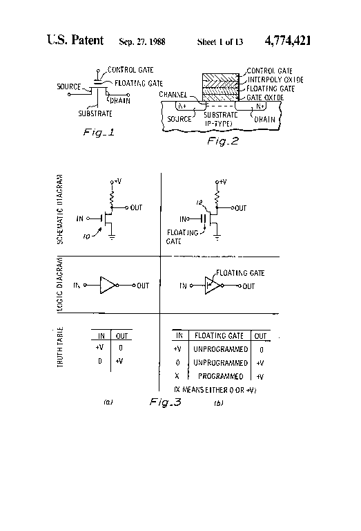
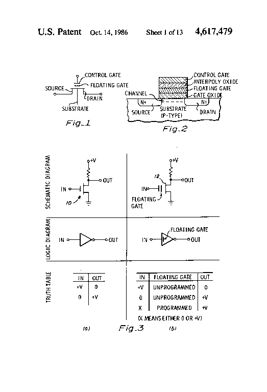
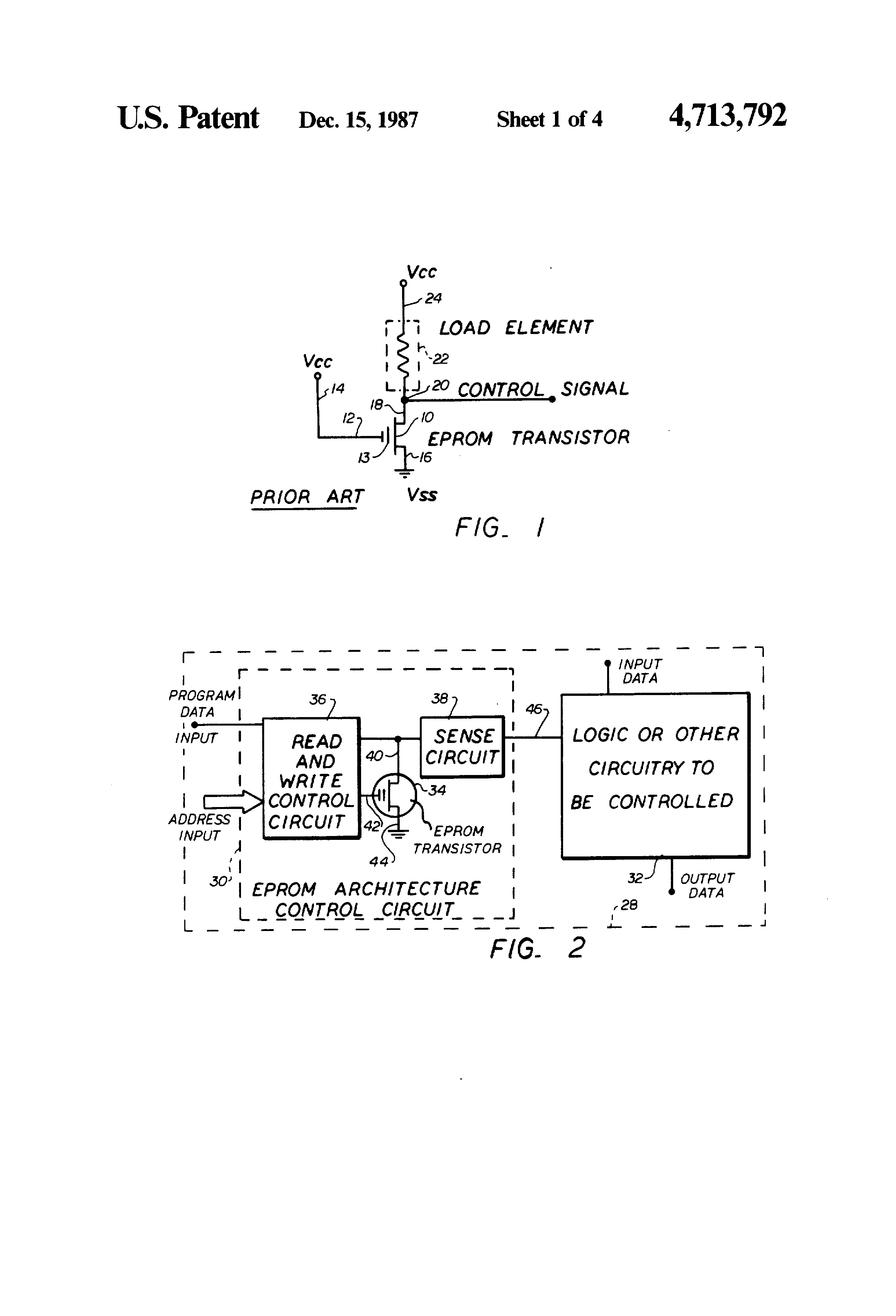
FIG. 1 is a schematic diagram illustrating an EPROM transistor configured for use as an architectural control element;

FIG. 2 is a generalized block diagram showing the basic components of an architecture control circuit in accordance with the present invention;

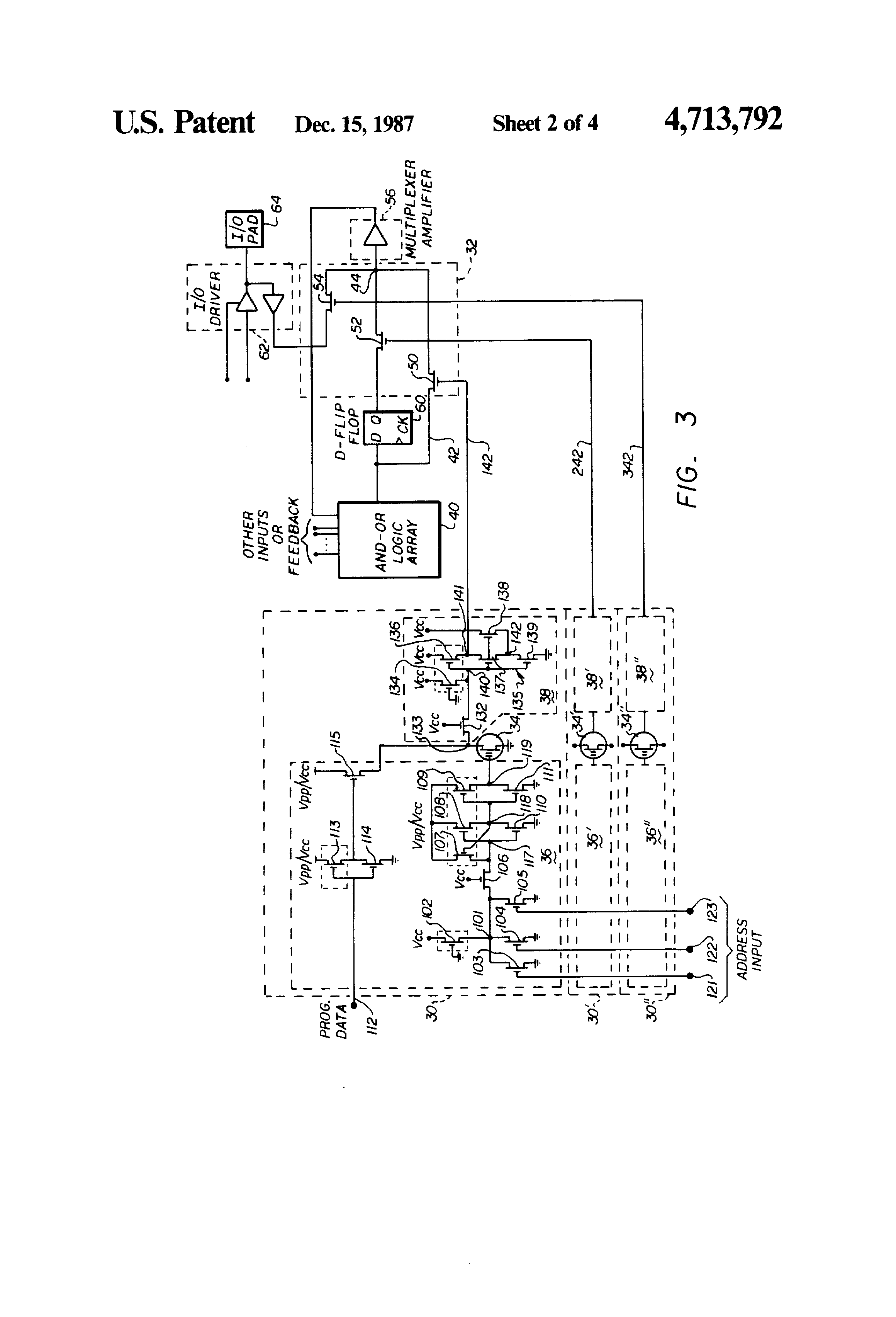
FIG. 3 is a schematic circuit illustrating specific embodiments of the present invention used in a transmission gate multiplexor circuit;

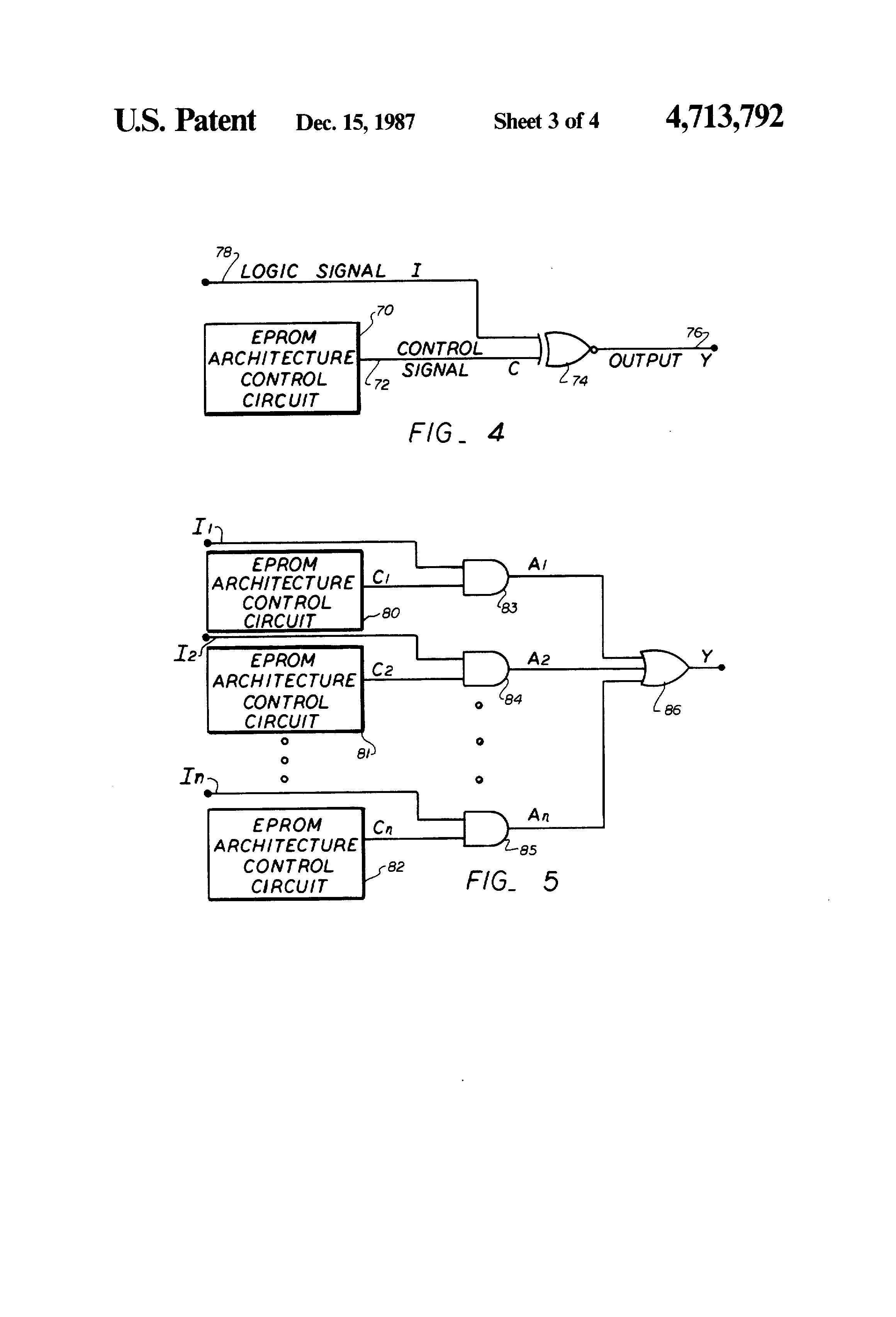
FIG. 4 is a diagram schematically illustrating use of the present invention in an inversion control circuit;

FIG. 5 is a diagram schematically illustrating use of the present invention in a digital multiplexer circuit;

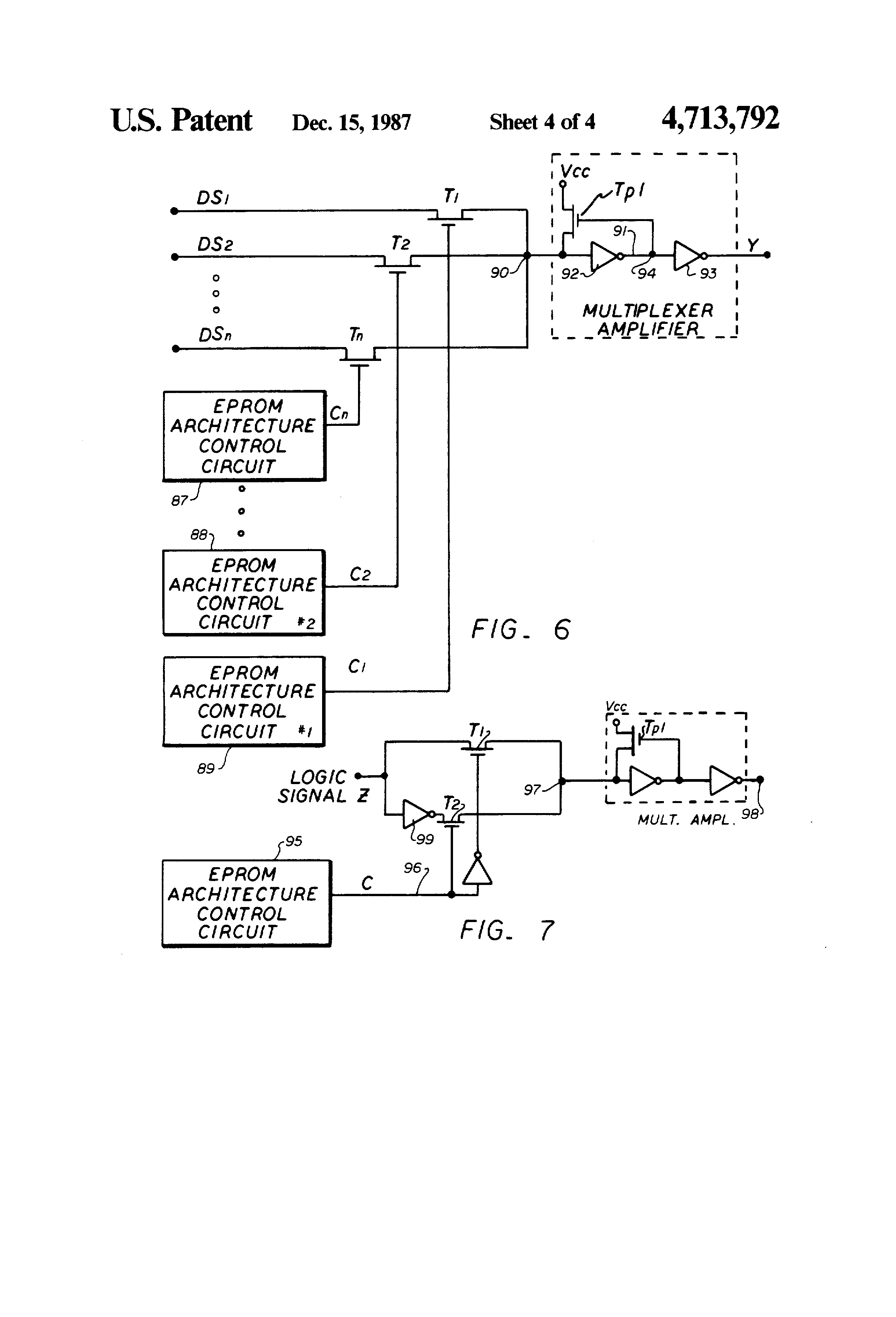
FIG. 6 is a diagram schematically illustrating use of the present invention in a transmission gate multiplexer circuit; and

FIG. 7 is a diagram schematically illustrating use of the present invention in a transmission gate inversion control circuit.

DETAILED DESCRIPTION OF THE PREFERRED EMBODIMENT

By way of introduction, a schematic diagram is shown in FIG. 1 of a well known prior art EPROM switching circuit which can be used in accordance with the present invention to generate a control signal. For purposes of this discussion an N-channel transistor is representationally shown, it being understood that a P-channel device could similarly be used. Furthermore, it is to be understood that the term EPROM is intended to include both EPROM and EEPROM devices. In FIG. 1, the EPROM transistor 10 has a gate 12 connected to an input terminal 14, a source 16 connected to circuit ground, and a drain 18 connected to an output node 20 and through a load resistor 22 to a supply voltage Vcc at a terminal 24.

If it is assumed that a floating gate 13 of the transistor is initially unprogrammed then the transistor can be expected to work as follows. Whenever a positive voltage greater than a certain threshold voltage (Vt) is applied to the control gate 12, a channel will be induced under the gate region of the transistor, which allows current to flow between the drain region and the source region. In a typical N-channenl floating gate device Vt is approximately 1.5 volts. The signals which are typically applied to a control gate are normally between 0 volts and 5 volts. With no input voltage applied to terminal 14, it will be appreciated that transistor 10 will be in a nonconducting or OFF state and node 20 will be pulled up through load element 22 to Vcc and thus be in a logic 1 state.

If on the other hand, an input voltage Vcc (nominally +5 volts) is applied to the gate 12, transistor 10 will be caused to conduct (turn ON) creating a current path between terminal 24 and circuit ground through load element 22. The load element 22 and transistor 10 are designed such that the control signal appearing at node 20, with transistor 10 conducting, will be less than the threshold voltage of a circuit to be controlled by the control signal. Thus, with transistor 10 turned ON, node 20 will be pulled toward ground potential and will thus be at a logic 0 state.

The effective threshold of transistor 10 will be changed by causing charges to be trapped on the floating gate 13. More particularly, electrons can be caused to flow to the floating gate 13 by applying a high voltage (typically 21 volts) to the control gate and the drain (by means not illustrated). When the high voltage is removed, charges will remain trapped on the floating gate 13 and cause the effective threshold of the device to be increased to a value greater than the voltage which would normally be applied to the control gate 12. The application of such high voltage and the subsequent charge trapping on the floating gate 13 is called "programming".

After transistor 10 has been programmed, if a 5 volt signal such as Vcc is applied to gate 12 no channel will be created between the source and drain, and no current will flow therebetween. Accordingly, transistor 10 will remain in its OFF condition causing node 20 to be pulled up to Vcc through load element 22. The control signal developed at node 20 will thus be greater than the threshold voltage of the circuit to be controlled, and will thus be considered to be at a logic 1 state.

The EPROM device can thus be thought of as a programmable switch. In the unprogrammed state, the switch opens and closes in response to the application of 0 volts or 5 volts, respectively, to the control gate 12. On the other hand, in the programmed state the switch will always be open regardless of whether 0 volts or 5 volts is applied to control gate 12. Under normal environmental conditions charges will stay trapped on the floating gate for very long periods of time, typically greater than 10 years.

Referring now to FIG. 2. of the drawing. A generalized block diagram is presented representatively showing a macrocell 28 including an architectural control circuit 30 connected to logic or other circuitry 32 to be controlled. In accordance with the present invention, circuit 30 is comprised of an EPROM (or EEPROM) transistor 34, Read and Write Control subcircuitry 36, and sense subcircuitry 38. Typically, the drain 40 and gate 42 of transistor 34 will be controlled by the Read and Write Control circuit 36, while the source 44 of the transistor is tied to ground. The sense circuit 38 couples the drain 40 to the circuitry 32 to be controlled. Furthermore, circuit 38 "senses" the programmed or unprogrammed state of transistor 34 and produces a corresponding logic 1 or logic 0 output signal at 46 which is used to control one or more subcircuits of circuitry 32.

Although illustrated as a single EPROM architecture control circuit 30, in the usual case a plurality of such circuits are combined to allow selective characterization of the operation of a particular logic or other circuit such as that depicted at 32. It will be appreciated, however, that the intended function of the several architecture control circuits is to input logic 1's and 0's to particular gates of the controlled circuit thus allowing the operational characteristics of such circuit to be tailored to fit a particular application.

Turning now to FIG. 3 of the drawing, a detailed schematic of an embodiment of the present invention is shown in an application in which EPROM control circuits are used to control a Transmission Gate Multiplexer circuit. In this embodiment, three Architectural Control circuits 30, 30' and 30" are shown in combination with multiplexing circuitry generally indicated at 32, which is in turn used to control the signal communication between the output, feedback and I/O of an AND-OR Logic Array 40. The overall architectural control system includes the three control circuits 30, 30' and 30" which respectively include the Read and Write Control subcircuits 36, 36' and 36" the EPROMs 34, 34' and 34" and the sense subcircuits 38, 38' and 38".

As mentioned, the circuitry 32 to be controlled is a three input transmission gate multiplexor consisting of switching transistors 50, 52 and 54 which forms part of an AND-OR array macrocell of the type disclosed in co-pending U.S. patent application Ser. No. 06/607,018 filed May 3, 1984 and assigned to the assignee of the present application. As illustrated, transistor 50 selectively connects the output of AND-OR array 40 to an amplifier 56 in a feedback loop, transistor 52 selectively connects the output of a D-flip-flop to amplifier 56, and transistor 54 selectively connects I/O pad 64 to amplifier 56 via an I/O driver 62. It will be appreciated that by means of the control circuits 30, any combination of the gates 50-54 may be actuated to specially configure the illustrated array.

Referring now to circuit 30, observe that control circuit 36 is comprised of a P-channel load transistor 102, three pull-down transistors 103, 104 and 105, the gates of which are connected to address terminals 121, 122, and 123, a blocking transistor 106, a level shifter or translator circuit consisting of three P-channel transistors 107, 108, and 109, and two N-channel transistors 110 and 111, the output of the translator circuit being connected to the gate of EPROM 34. Circuit 36 also includes a P-channel transistor 113 and an N-channel transistor 114 the gates which are connected to a program data input terminal 112 and invert an input applied thereto, and a transistor 115 the gate of which is connected to the drains of transistors 113 and 114. The source 116 of transistor 115 is connected to the drain of EPROM 34.

Sense circuit 38 includes a gating transistor 132, a P-channel load device 134 and a Schmidt Trigger Circuit 135 including a P-channel transistor 136 and N-channel transistors 137-139. The output node 141 of Schmidt trigger circuit 135 is coupled to the gate of transistor 50 of the multiplexing circuit 32.

Similarly, the other two (or more) control circuits consisting of read/write circuits 36' and 36", EPROM transistors 34' and 34" and sense circuits 38' and 38" are respectively coupled to the gates of transistors 52 and 54. It should be understood that each of the circuits 36, 36' and 36" share a common data line 112 and common address lines 121-123. The use of inverters to interface appropriate address lines to 36' and 36" allow selection of a particular one of the EPROMs 34', 34" to be programmed by the data signal input on the program data input line.

Operation of the illustrated circuit may be explained as follows:

Assume initially that the EPROM transistors 34, 34' and 34" are in their erased state and it is desired to write a value to the floating gates. For purposes of this discussion a description of the "Write" operation for only transistor 34 will be given although such operations for 34' and 34" will be similar. During writing, the Vpp/Vcc line is switched to Vpp (typically 21 volts). Transistor 102 serves as a load transistor and transistors 103, 104 and 105 are pull down transistors making up a 3 input NOR gate. If the address inputs 121, 122, and 123 are all logic 0 then the output of the NOR gate at node 101 will be a logic 1. With Vcc at the gate of transistor 106 it will be rendered conductive and the logic 1 will be passed to node 117. Because the gate of transistor 106 is connected to Vcc, the initial node voltage at 117 will be Vcc-Vt, or approximately 4 volts. This will be high enough to turn transistor 110 ON, but not enough to turn P-channel transistor 108 OFF.

With transistor 110 ON, node 118 begins to be pulled toward ground. This turns P-channel transistor 107 ON and pulls node 117 toward Vpp which turns transistor 108 fully OFF. With node 118 at ground, N-channel transistor 111 is OFF and P-channel transistor 109 is ON causing node 119 to be pulled up to Vpp which is the desired programming gate voltage for EPROM transistor 38. Line 112 contains the data to be programmed. If the data on line 112 is a logic 0, then transistor 115 will be turned ON and the EPROM transistor 34 will be programmed as the drain 133 of transistor 34 is pulled to Vpp through N-channel transistor 115. If the signal input on line 112 is a logic 1 transistor 115 will remain OFF and the EPROM transistor will not be programmed.

Once the EPROM transistor 34 is programmed, it can be sensed by Sense circuit 38. During the normal operation (after programming), line 112 is forced to a logic 1, Vpp/Vcc is forced to Vcc and lines 121, 122 and 123 are forced to logic 0, thus node 119 will be at a Vcc level.

The Sense circuit works as follows: First, assume that transistor 34 is in its erased state. With 5 volts applied to its gate it will be turned ON. P-channel transistor 134 acts as a load element for transistor 34 through pass gate transistor 132. The sizes of transistors 132, 134 and EPROM 34 are chosen such that node 40 will be near ground (logic 0) when EPROM 34 is in its erased state. This level is sensed by Schmidt trigger circuit 135. A logic 0 on node 140 produces a logic 1 on node 141. Thus, an erased EPROM (unprogrammed) transistor will be sensed as a logic 1.

Next, assume that the EPROM 34 has been programmed and is in its OFF state. Then with 5 volts on its gate it will still be in an OFF configuration. This will be sensed by the Schmidt trigger and a logic 0 will be output at 141. Thus, a programmed EPROM transistor produces a logic 0 at node 141.

In a similar manner, EPROM transistors 34' and 34" can be programmed by their respective Read/Write Control circuits 36' and 36". Having programmed EPROM transistors 34 34' and 34", the control signals developed on lines 142, 242 and 342 are used to control the transmission multiplexer (TMUX). Typically, in a TMUX only one path is active. For example, assume the gate of transistor 50 is at a logic 1, and the gates of transistors 52 and 54 are at logic 0, then data from the AND/OR Logic Array 40 will be passed via line 42 through transistor 50 to node 44 where it will be amplified by the multiplex amplifier 56 and (in this illustration) passed back to the AND/OR Array 40. If transistor 52 had been selected (rather than 50) than data from the D flip-flop 60 would have been fed back to the AND/OR Array 40. If transistor 54 had been selected, then I/O pad data would have been passed through amplifier 56 to the AND/OR Array 40.

Many other circuits can also be controlled by EPROM architecture control circuits of the type described. For example, FIG. 4 shows an inversion control circuit (of the type disclosed by Brickman et al in "Programmable Logic Array Enhancement", IBM Tech. Disclosure Bulletin, p. 583, Vol. 19, No. 2, July 1976). in which an EPROM architecture control circuit 70 in accordance with the present invention generates a control signal C on a control line 72. By applying the control signal C to one input of an exclusive NOR gate 74, the output signal Y at 76 will be either the same as, or the logical inversion of, the logic signal I input at 78. The following truth table illustrates the application:

It will thus be appreciated that when C=0, Y=I, and when C=1, Y=I.

FIG. 5 illustrates a digital multiplexer in which a plurality of EPROM architecture control circuits 80, 81 and 82, provide control signals C1, C2, . . . Cn for the multiplexing circuitry consisting of AND gates 83, 84 and 85, the outputs of which are fed into an OR gate 86. The output Y of OR gate 86 will be the logical OR of all signals I1, I2, . . . . In whose control signals C1, C2 . . . Cn are set to logic 1. The logic equation for this circuit is:

By way of example, if C1=0, C2=1, and C3 through Cn=0, then Y=I2.

In FIG. 6 another version of a multiplexer circuit is shown wherein pass gates T1, T2 . . . Tn are controlled by EPROM architecture control circuits 87, 88, and 89. In this type of circuit, normally referred to as a Transmission Gate Multiplexer, only one of the pass gates can be enabled or a conflict will exist at node 90 and the output signal Y will be indeterminate. Assuming only one control signal, for example C1, is at a logic 1 state then the circuit works as follows: Transistor T1 is turned ON and transistors T2 . . . Tn are turned OFF. Signal DS1 will then be passed to node 90. If DS1 is a logic 0, then node 90, will also be pulled to logic 0, and the output 91 of inverter 92 will be at logic 1, which turns OFF transistor TP1. The output Y from inverter 93 will thus be at logic 0.

Next, assume DS1 goes to a logic 1. Initially node 90 can only go as high as Vcc-Vt (assuming the logic 1 level of C1 is Vcc). Inverter 92 is designed such that Vcc-Vt is enough to begin pulling node 94 low. This will turn Tp1 ON and pull node 90 to Vcc. Output Y will then go to logic 1 in response to a logic 0 at node 94.

In FIG. 7 a special case of the transmission gate multiplexer is shown in which an EPROM architectural control circuit 95 is used to accomplish inversion control. In this circuit, two transmission gates T1 and T2 are controlled by an EPROM architecture control bit C. Depending upon the state of the invert control line 96, either T1 will be ON and T2 will be OFF or T1 will be OFF and T2 will be ON. If T1 is ON, the logic signal Z will be passed to node 97 and thereafter through the multiplexer amplifier (as in FIG. 6) to the output 98. In this case, the output 98 will have the same logical values as input Z. If, on the other hand, T2 is ON, the logic signal Z will be inverted by the inverter gate 99 and passed to node 97 and thence to the output 98. In this case, output 98 will be the logical complement of the input signal Z. Thus, the circuit shown in FIG. 7 acts as a programmable inverter under control of an EPROM control bit.

Although the present invention has been described above with regard to a particular preferred embodiment which can be utilized as the control means for several different types of circuits, it is contemplated that other circuits and embodiments will become apparent to those skilled in the art after having read the above disclosure. It is therefore intended that the following claims be interpreted as covering all such circuits and embodiments as fall within the true spirit and scope of the invention.
Claims (19)

  1. A programmable macrocell in an integrated circuit device comprising: electronic circuit means responsive to a program control signal and operative to perform a particular operation selected by said control signal on an input data signal and to develop a commensurate output data signal, said electronic circuit means including an inversion control circuit having exclusive NOR gate means with one input thereof receiving said control signal and another input thereof receiving said input data signal; and architecture control means including one or more architecture control circuits each having a programmable EPROM device having gate, drain and source electrodes and which when programmed generates a logic signal of a first state and when unprogrammed generates a logic signal of a second state, read and write control means connected to said EPROM device and responsive to an input program data signal and a corresponding address signal and operative to program said EPROM device by applying a programming potential thereto, and sense means connected to said EPROM device for sensing the programmed or unprogrammed state of said EPROM device and for developing a commensurate control signal for input to said inversion control circuit, whereby in response to said control signal said inversion control circuit causes an input data signal to be inverted when an associated EPROM device is in said first state and to be not inverted when said EPROM device is in said second state.
  2. A programmable macrocell as recited in claim 1 wherein said read/write control means includes a programming circuit responsive to said program data signals and operative to apply said programming potential to the drain electrode of said EPROM device, a NOR gate responsive to said address signal and operative to develop a logic output, and switching means responsive to said logic output of said NOR gate and operative to couple said programming potential to the gate electrode of said EPROM device to effect programming thereof.
  3. A programmable macrocell as recited in claim 2 wherein said architecture control circuits are implemented using EEPROM devices rather than EPROM devices.
  4. A programmable macrocell as recited in claim 2 wherein said programming circuit includes a first transistor switching element for coupling said programming potential to the drain electrode of said EPROM device and an inverting circuit coupled to the gate electrode thereof for inverting said program data signal.
  5. A programmable macrocell as recited in claim 4 wherein said architecture control circuits are implemented using EEPROM devices rather than EPROM devices.
  6. A programmable macrocell as recited in claim 4 wherein said sense means includes a Schmidt trigger circuit coupled to the drain electrode of said EPROM device and operative to develop a control signal corresponding to the state of the logic signal generated by said EPROM device.
  7. A programmable macrocell as recited in claim 6 wherein said architecture control circuits are implemented using EEPROM devices rather than EPROM devices.
  8. A programmable macrocell as recited in claim 1 wherein said architecture control circuits are implemented using EEPROM devices rather than EPROM devices.
  9. A programmable macrocell in an integrated circuit device comprising: architecture control means including a plurality of architecture control circuits each having a programmable EPROM device including gate, drain and source electrodes which when programmed generates a logic signal of a first state and when unprogrammed generates a logic signal of a second state, read and write control means connected to said EPROM device and responsive to an input program data signal and a corresponding address signal and operative to program said EPROM device by applying a programming potential thereto, and sense means connected to said EPROM device for sensing the programmed or unprogrammed state of said EPROM device and for developing a commensurate control signal; and electronic circuit means responsive to said control signals and operative to perform particular operations selected by said control signals on input data signals and to develop commensurate output data signals, said electronic circuit means including a digital multiplexer means having a plurality of AND gates each of which receives at least one input data signal and a control signal developed by said architecture control means, the outputs of said AND gates being ORed together in an output OR gate which in turn develops an output signal corresponding to one of said input data signals as selected by a particular one of said control signals.
  10. A programmable macrocell as recited in claim 9 wherein said read and write control means includes a programming circuit responsive to said program data signal and operative to apply said programming potential to the drain electrode of said EPROM device, a NOR gate responsive to said address signal and operative to develop a logic output, and switching means responsive to said logic output of said NOR gate and operative to couple said programming potential to the gate electrode of said EPROM device to effect programming thereof.
  11. A programmable macrocell as recited in claim 10 wherein said programming circuit includes a first transistor switching element for coupling said programming potential to the drain of said EPROM device and an inverting circuit coupled to the gate electrode thereof for inverting said program data signal.
  12. A programmable macrocell as recited in claim 11 wherein said sense means includes a Schmidt trigger circuit coupled to the drain electrode of said EPROM device and operative to develop a control signal corresponding to the state of the logic signal generated by said EPROM device.
  13. An integrated circuit device comprising: electronic logic circuit means responsive to at least one control signal and operable to perform a particular logic function on at least one input data signal to generate at least one commensurate output signal; and programmable control means for causing said logic circuit means to have particular circuit configurations, and including: a first reprogrammable memory device which may be programed to generate either a logic signal of a first state or a logic signal of a second state; a first programming means connected to said first reprogrammable memory device and responsive to input program data signals and a corresponding address signal and operative to program said first reprogrammable memory device by applying a programming potential thereto; a first sense means connected to said first reprogrammable memory device for sensing the state of the logic signal generated by said first reprogrammable memory device and for developing a commensurate first control signal for controlling said logic circuit means.
  14. An integrated circuit device as recited in claim 13 wherein said electronic logic circuit means includes an exclusive NOR gate.
  15. An integrated circuit device as recited in claim 14 wherein said first memory device is an EPROM transistor.
  16. An integrated circuit device as recited in claim 14 wherein said first memory device is an EEPROM transistor.
  17. An integrated circuit device as recited in claim 13 wherein said programmable means further includes a second reprogrammable memory device which may be programmed to generate either a logic signal of a first state or a logic signal of a second state; a second programming means connected to said second reprogrammable memory device and responsive to input program data signals and a corresponding address signal and operative to program said second reprogrammable memory device by applying a programming potential thereto; a second sense means connected to said second reprogrammable memory device for sensing the state of the logic signal generated by said second reprogrammable memory device and for developing a commensurate second control signal for controlling said logic circuit means; and wherein said logic circuit means includes a first AND gate having a first input for receiving a first input data signal, and a second input for receiving said first control signal and operative to generate a first intermediate data signal; at least a second AND gate having a first input for receiving a second input data signal, and a second input for receiving said second control signal and operative to generate a second intermediate data signal; and an OR gate responsive to said first and second intermediate data signals and operative to generate said output signal.
  18. An integrated circuit device as rectied in claim 17 wherein said first and second reprogrammable memory devices are EPROM transistors.
  19. An integrated circuit device as recited in claim 17 wherein said first and second reprogrammable memory devices are EEPROM transistors.

Publications

Related applications (9)

  1. US06/742,089

    Priority application

  2. DE8686107450T

    Priority application

  3. AT86107450T

    Priority application

  4. EP86107450A

    Priority application

  5. JP61127413A

    Priority application

  6. US06/907,075

    Priority application

  7. JP007239U

    Priority application

  8. US06/742,089

    Claims priority

  9. US06/742,089

    Patent family

Record timeline

  1. First worldwide family litigation filed

  2. Assigned to ALTERA CORPORATION 3525 MONROE STREET, SANTA CLARA CA 95051 A CORP OF CA

  3. Priority to US06/742,089

  4. Application filed by Altera Corp

  5. Priority to DE8686107450T

  6. Priority to AT86107450T

  7. Priority to EP86107450A

  8. Priority to JP61127413A

  9. Priority to US06/907,075

  10. Publication of US4713792A

  11. Application granted

  12. Priority to JP007239U

  13. Assigned to ALTERA CORPORATION, A DELAWARE CORPORATION

  14. Anticipated expiration

  15. Expired - LifetimeCurrent

Legal events

  1. AS

    Assignment

    Owner name: ALTERA CORPORATION 3525 MONROE STREET, SANTA CLARA

    Free format text: ASSIGNMENT OF ASSIGNORS INTEREST.;ASSIGNORS:HARTMANN, ROBERT F.;CHAN, YIU-FAI;FRANKOVICH, ROBERT J.;AND OTHERS;REEL/FRAME:004414/0853

    Effective date: 19850606

  2. STCF

    Information on status: patent grant

    Free format text: PATENTED CASE

  3. FEPP

    Fee payment procedure

    Free format text: PAT HLDR NO LONGER CLAIMS SMALL ENT STAT AS SMALL BUSINESS (ORIGINAL EVENT CODE: LSM2); ENTITY STATUS OF PATENT OWNER: LARGE ENTITY

  4. FPAY

    Fee payment

    Year of fee payment: 4

  5. FEPP

    Fee payment procedure

    Free format text: PAYOR NUMBER ASSIGNED (ORIGINAL EVENT CODE: ASPN); ENTITY STATUS OF PATENT OWNER: LARGE ENTITY

  6. FPAY

    Fee payment

    Year of fee payment: 8

  7. AS

    Assignment

    Owner name: ALTERA CORPORATION, A DELAWARE CORPORATION, CALIFO

    Free format text: MERGER;ASSIGNOR:ALTERA CORPORATION, A CALIFORNIA CORPORATION;REEL/FRAME:009015/0336

    Effective date: 19970325

  8. FPAY

    Fee payment

    Year of fee payment: 12

Patent citations (2)

  1. US3921146A

    Programmable data processor and controller system

    Gen Electric · November 18, 1975 · Examiner cited

  2. US4524428A

    Modular input-programmable logic circuits for use in a modular array processor

    Hughes Aircraft Company · June 18, 1985 · Examiner cited

Cited by (257)

  1. US5764078A

    Family of multiple segmented programmable logic blocks interconnected by a high speed centralized switch matrix

    Advanced Micro Devices, Inc. · June 9, 1998 · Examiner cited

  2. US5869981A

    High density programmable logic device

    Advanced Micro Devices, Inc. · February 9, 1999 · Examiner cited

  3. US5436514A

    High speed centralized switch matrix for a programmable logic device

    Advanced Micro Devices, Inc. · July 25, 1995 · Examiner cited

  4. US5612631A

    An I/O macrocell for a programmable logic device

    Advanced Micro Devices, Inc. · March 18, 1997 · Examiner cited

  5. US5426335A

    Pinout architecture for a family of multiple segmented programmable logic blocks interconnected by a high speed centralized switch matrix

    Advanced Micro Devices, Inc. · June 20, 1995 · Examiner cited

  6. US5784637A

    Single-chip semiconductor integrated circuit device and microcomputer integrated on a semiconductor chip

    Hitachi, Ltd. · July 21, 1998 · Examiner cited

  7. US5428808A

    Single-chip microcomputer

    Hitachi, Ltd. · June 27, 1995 · Examiner cited

  8. US5321845A

    Single-chip microcomputer including non-volatile memory elements

    Hitachi, Ltd. · June 14, 1994 · Examiner cited

  9. US5105388A

    Programmable logic device including verify circuit for macro-cell

    Fujitsu Limited · April 14, 1992 · Examiner cited

  10. US4912342A

    Programmable logic device with array blocks with programmable clocking

    Altera Corporation · March 27, 1990 · Examiner cited

  11. US4903223A

    Programmable logic device with programmable word line connections

    Altera Corporation · February 20, 1990 · Examiner cited

  12. US4864161A

    Multifunction flip-flop-type circuit

    Altera Corporation · September 5, 1989 · Examiner cited

  13. US4871930A

    Programmable logic device with array blocks connected via programmable interconnect

    Altera Corporation · October 3, 1989 · Examiner cited

  14. US4899070A

    Bit line sense amplifier for programmable logic devices

    Altera Corporation · February 6, 1990 · Examiner cited

  15. US4899067A

    Programmable logic devices with spare circuits for use in replacing defective circuits

    Altera Corporation · February 6, 1990 · Examiner cited

  16. US4930107A

    Method and apparatus for programming and verifying programmable elements in programmable devices

    Altera Corporation · May 29, 1990 · Examiner cited

  17. US5511211A

    Method for flexibly developing a data processing system comprising rewriting instructions in non-volatile memory elements after function check indicates failure of required functions

    Hitachi, Ltd. · April 23, 1996 · Examiner cited

  18. US4906870A

    Low power logic array device

    Atmel Corporation · March 6, 1990 · Examiner cited

  19. US4940909A

    Configuration control circuit for programmable logic devices

    Plus Logic, Inc. · July 10, 1990 · Examiner cited

  20. US5200920A

    Method for programming programmable elements in programmable devices

    Altera Corporation · April 6, 1993 · Examiner cited

  21. US5274778A

    EPROM register providing a full time static output signal

    National Semiconductor Corporation · December 28, 1993 · Examiner cited

  22. US5373510A

    Test circuit of input architecture of erasable and programmable logic device

    Hyundai Electronics Co., Ltd. · December 13, 1994 · Examiner cited

  23. US5485103A

    Programmable logic array with local and global conductors

    Altera Corporation · January 16, 1996 · Examiner cited

  24. US6759870B2

    Programmable logic array integrated circuits

    Altera Corporation · July 6, 2004

  25. US5485102A

    Programmable logic devices with spare circuits for replacement of defects

    Altera Corporation · January 16, 1996 · Examiner cited

  26. US5483178A

    Programmable logic device with logic block outputs coupled to adjacent logic block output multiplexers

    Altera Corporation · January 9, 1996 · Examiner cited

  27. US6181162B1

    Programmable logic device with highly routable interconnect

    Altera Corporation · January 30, 2001

  28. USRE38651E1

    Variable depth and width memory device

    Altera Corporation · November 9, 2004 · Examiner cited

  29. US6122720A

    Coarse-grained look-up table architecture

    Altera Corporation · September 19, 2000 · Examiner cited

  30. US5815726A

    Coarse-grained look-up table architecture

    Altera Corporation · September 29, 1998 · Examiner cited

  31. US5850365A

    Sense amplifier with individually optimized high and low power modes

    Altera Corporation · December 15, 1998 · Examiner cited

  32. US5525917A

    Sense amplifier with feedback and stabilization

    Altera Corporation · June 11, 1996 · Examiner cited

  33. US5598109A

    Programmable logic array device with grouped logic regions and three types of conductors

    Altera Corporation · January 28, 1997 · Examiner cited

  34. US5537057A

    Programmable logic array device with grouped logic regions and three types of conductors

    Altera Corporation · July 16, 1996 · Examiner cited

  35. US5963049A

    Programmable logic array integrated circuit architectures

    Altera Corporation · October 5, 1999 · Examiner cited

  36. US6392438B1

    Programmable logic array integrated circuit devices

    Altera Corporation · May 21, 2002

  37. US6184705B1

    Techniques for programming programmable logic array devices

    Altera Corporation · February 6, 2001

  38. US6191608B1

    Techniques for programming programmable logic array devices

    Altera Corporation · February 20, 2001

  39. US5680061A

    Techniques for programming programmable logic array devices

    Altera Corporation · October 21, 1997 · Examiner cited

  40. US5689195A

    Programmable logic array integrated circuit devices

    Altera Corporation · November 18, 1997 · Examiner cited

  41. US6204688B1

    Programmable logic array integrated circuit devices with interleaved logic array blocks

    Altera Corporation · March 20, 2001

  42. US5986470A

    Programmable logic array integrated circuit devices

    Altera Corporation · November 16, 1999 · Examiner cited

  43. US5705939A

    Programmable logic array integrated circuits with segmented, selectively connectable, long interconnection conductors

    Altera Corporation · January 6, 1998 · Examiner cited

  44. US5717901A

    Variable depth and width memory device

    Altera Corporation · February 10, 1998 · Examiner cited

  45. US6259272B1

    Programmable logic array integrated circuit architectures

    Altera Corporation · July 10, 2001

  46. US5850152A

    Programmable logic array integrated circuit devices

    Altera Corporation · December 15, 1998 · Examiner cited

  47. US6278291B1

    Programmable logic array devices with interconnect lines of various lengths

    Altera Corporation · August 21, 2001

  48. US6366121B2

    Programmable logic array integrated circuit architectures

    Altera Corporation · April 2, 2002

  49. US5543732A

    Programmable logic array devices with interconnect lines of various lengths

    Altera Corporation · August 6, 1996 · Examiner cited

  50. US5592106A

    Programmable logic array integrated circuits with interconnection conductors of overlapping extent

    Altera Corporation · January 7, 1997 · Examiner cited

  51. US6396304B2

    Programmable logic array integrated circuits with blocks of logic regions grouped into super-blocks

    Altera Corporation · May 28, 2002

  52. US5936425A

    Tri-statable input/output circuitry for programmable logic

    Altera Corporation · August 10, 1999 · Examiner cited

  53. US5541530A

    Programmable logic array integrated circuits with blocks of logic regions grouped into super-blocks

    Altera Corporation · July 30, 1996 · Examiner cited

  54. US5909126A

    Programmable logic array integrated circuit devices with interleaved logic array blocks

    Altera Corporation · June 1, 1999 · Examiner cited

  55. US5796267A

    Tri-Statable input/output circuitry for programmable logic

    Altera Corporation · August 18, 1998 · Examiner cited

  56. US5900743A

    Programmable logic array devices with interconnect lines of various lengths

    Altera Corporation · May 4, 1999 · Examiner cited

  57. US6154055A

    Programmable logic array integrated circuit devices

    Altera Corporation · November 28, 2000 · Examiner cited

  58. US5850151A

    Programmable logic array intergrated circuit devices

    Altera Corporation · December 15, 1998 · Examiner cited

  59. US5614840A

    Programmable logic array integrated circuits with segmented, selectively connectable, long interconnection conductors

    Altera Corporation · March 25, 1997 · Examiner cited

  60. US6815981B2

    Programmable logic array integrated circuit devices

    Altera Corporation · November 9, 2004

  61. US6127846A

    Programmable logic array devices with interconnect lines of various lengths

    Altera Corporation · October 3, 2000 · Examiner cited

  62. US5659717A

    Methods for partitioning circuits in order to allocate elements among multiple circuit groups

    Altera Corporation · August 19, 1997 · Examiner cited

  63. US5812450A

    Nonvolatile SRAM cells and cell arrays

    Altera Corporation · September 22, 1998 · Examiner cited

  64. US5581501A

    Nonvolatile SRAM cells and cell arrays

    Altera Corporation · December 3, 1996 · Examiner cited

  65. US5565793A

    Programmable logic array integrated circuit devices with regions of enhanced interconnectivity

    Altera Corporation · October 15, 1996 · Examiner cited

  66. US6049225A

    Input/output interface circuitry for programmable logic array integrated circuit devices

    Altera Corporation · April 11, 2000 · Examiner cited

  67. US5764080A

    Input/output interface circuitry for programmable logic array integrated circuit devices

    Altera Corporation · June 9, 1998 · Examiner cited

  68. US5631576A

    Programmable logic array integrated circuit devices with flexible carry chains

    Altera Corporation · May 20, 1997 · Examiner cited

  69. US5821773A

    Look-up table based logic element with complete permutability of the inputs to the secondary signals

    Altera Corporation · October 13, 1998 · Examiner cited

  70. US5642480A

    Method and apparatus for enhanced security of a data processor

    Motorola, Inc. · June 24, 1997 · Examiner cited

  71. US5729495A

    Dynamic nonvolatile memory cell

    Altera Corporation · March 17, 1998 · Examiner cited

  72. US5740110A

    Dynamic nonvolatile memory cell

    Altera Corporation · April 14, 1998 · Examiner cited

  73. US5898630A

    Dynamic nonvolatile memory cell

    Altera Corporation · April 27, 1999 · Examiner cited

  74. US5805516A

    Dynamic nonvolatile memory cell

    Altera Corporation · September 8, 1998 · Examiner cited

  75. USRE40011E1

    System for coupling programmable logic device to external circuitry which selects a logic standard and uses buffers to modify output and input signals accordingly

    Altera Corporation · January 22, 2008

  76. US5744991A

    System for distributing clocks using a delay lock loop in a programmable logic circuit

    Altera Corporation · April 28, 1998 · Examiner cited

  77. US6130552A

    Programmable logic integrated circuit with on-chip DLL or PLL for clock distribution

    Altera Corporation · October 10, 2000 · Examiner cited

  78. US5963069A

    System for distributing clocks using a delay lock loop in a programmable logic circuit

    Altera Corporation · October 5, 1999 · Examiner cited

  79. US5970255A

    System for coupling programmable logic device to external circuitry which selects a logic standard and uses buffers to modify output and input signals accordingly

    Altera Corporation · October 19, 1999 · Examiner cited

  80. US5592102A

    Means and apparatus to minimize the effects of silicon processing defects in programmable logic devices

    Altera Corporation · January 7, 1997 · Examiner cited

  81. US5670895A

    Routing connections for programmable logic array integrated circuits

    Altera Corporation · September 23, 1997 · Examiner cited

  82. US5825197A

    Means and apparatus to minimize the effects of silicon processing defects in programmable logic devices

    Altera Corporation · October 20, 1998 · Examiner cited

  83. US5555214A

    Apparatus for serial reading and writing of random access memory arrays

    Altera Corporation · September 10, 1996 · Examiner cited

  84. US5793246A

    High voltage pump scheme incorporating an overlapping clock

    Altera Corporation · August 11, 1998 · Examiner cited

  85. USRE37060E1

    Apparatus for serial reading and writing of random access memory arrays

    Altera Corporation · February 20, 2001

  86. US6236260B1

    High voltage pump scheme incorporating an overlapping clock

    Altera Corporation · May 22, 2001

  87. US5672985A

    Programmable logic array integrated circuits with carry and/or cascade rings

    Altera Corporation · September 30, 1997 · Examiner cited

  88. US5767734A

    High-voltage pump with initiation scheme

    Altera Corporation · June 16, 1998 · Examiner cited

  89. US6239613B1

    Tristate structures for programmable logic devices

    Altera Corporation · May 29, 2001

  90. US6882177B1

    Tristate structures for programmable logic devices

    Altera Corporation · April 19, 2005

  91. US5894228A

    Tristate structures for programmable logic devices

    Altera Corporation · April 13, 1999 · Examiner cited

  92. US5691653A

    Product term based programmable logic array devices with reduced control memory requirements

    Altera Corporation · November 25, 1997 · Examiner cited

  93. US6045252A

    Methods for allocating circuit design portions among physical circuit portions

    Altera Corporation · April 4, 2000 · Examiner cited

  94. US5768372A

    Method and apparatus for securing programming data of a programmable logic device

    Altera Corporation · June 16, 1998 · Examiner cited

  95. US5915017A

    Method and apparatus for securing programming data of programmable logic device

    Altera Corporation · June 22, 1999 · Examiner cited

  96. US6366498B1

    Nonvolatile configuration cells and cell arrays

    Altera Corporation · April 2, 2002

  97. US6226201B1

    Techniques to configure nonvolatile cells and cell arrays

    Altera Corporation · May 1, 2001

  98. US6005806A

    Nonvolatile configuration cells and cell arrays

    Altera Corporation · December 21, 1999 · Examiner cited

  99. US6532170B1

    Nonvolatile configuration cells and cell arrays

    Altera Corporation · March 11, 2003

  100. US6052309A

    Nonvolatile configuration cells and cell arrays

    Altera Corporation · April 18, 2000 · Examiner cited

  101. US6295230B1

    Nonvolatile configuration cells and cell arrays

    Altera Coporation · September 25, 2001

  102. US5694058A

    Programmable logic array integrated circuits with improved interconnection conductor utilization

    Altera Corporation · December 2, 1997 · Examiner cited

  103. US5835998A

    Logic cell for programmable logic devices

    Altera Corporation · November 10, 1998 · Examiner cited

  104. US5872463A

    Routing in programmable logic devices using shared distributed programmable logic connectors

    Altera Corporation · February 16, 1999 · Examiner cited

  105. US6184706B1

    Logic device architecture and method of operation

    Altera Corporation · February 6, 2001

  106. US6492834B1

    Programmable logic device with highly routable interconnect

    Altera Corporation · December 10, 2002

  107. US5869979A

    Technique for preconditioning I/Os during reconfiguration

    Altera Corporation · February 9, 1999 · Examiner cited

  108. US6208162B1

    Technique for preconditioning I/Os during reconfiguration

    Altera Corporation · March 27, 2001

  109. US6294928B1

    Programmable logic device with highly routable interconnect

    Altera Corporation · September 25, 2001

  110. US6414514B1

    Logic device architecture and method of operation

    Altera Corporation · July 2, 2002

  111. US6246260B1

    Programmable logic integrated circuit architecture incorporating a global shareable expander

    Altera Corporation · June 12, 2001

  112. US6271680B1

    Logic element for a programmable logic integrated circuit

    Altera Corporation · August 7, 2001

  113. US6275065B1

    Programmable logic integrated circuit architecture incorporating a lonely register

    Altera Corporation · August 14, 2001

  114. US6107822A

    Logic element for a programmable logic integrated circuit

    Altera Corporation · August 22, 2000 · Examiner cited

  115. US5986465A

    Programmable logic integrated circuit architecture incorporating a global shareable expander

    Altera Corporation · November 16, 1999 · Examiner cited

  116. US6359469B1

    Logic element for a programmable logic integrated circuit

    Altera Corporation · March 19, 2002

  117. US5939790A

    Integrated circuit pad structures

    Altera Corporation · August 17, 1999 · Examiner cited

  118. US6624524B1

    Laser alignment target

    Altera Corporation · September 23, 2003

  119. US6002182A

    Laser alignment target

    Altera Corporation · December 14, 1999 · Examiner cited

  120. US6573138B1

    Nonvolatile memory cell with low doping region

    Altera Corporation · June 3, 2003

  121. US6828620B2

    Nonvolatile memory cell with low doping region

    Altera Corporation · December 7, 2004

  122. US20030197218A1

    Nonvolatile memory cell with low doping region

    Altera Corporation · October 23, 2003 · Examiner cited

  123. US5998295A

    Method of forming a rough region on a substrate

    Altera Corporation · December 7, 1999 · Examiner cited

  124. US6122209A

    Method of margin testing programmable interconnect cell

    Altera Corporation · September 19, 2000 · Examiner cited

  125. US5949710A

    Programmable interconnect junction

    Altera Corporation · September 7, 1999 · Examiner cited

  126. US5977791A

    Embedded memory block with FIFO mode for programmable logic device

    Altera Corporation · November 2, 1999 · Examiner cited

  127. US6242946B1

    Embedded memory block with FIFO mode for programmable logic device

    Altera Corporation · June 5, 2001

  128. US6344758B1

    Interface for low-voltage semiconductor devices

    Altera Corporation · February 5, 2002

  129. US6118302A

    Interface for low-voltage semiconductor devices

    Altera Corporation · September 12, 2000 · Examiner cited

  130. US6583646B1

    Overvoltage-tolerant interface for integrated circuits

    Altera Corporation · June 24, 2003

  131. US6563343B1

    Circuitry for a low internal voltage

    Altera Corporation · May 13, 2003

  132. US6342794B1

    Interface for low-voltage semiconductor devices

    Altera Corporation · January 29, 2002

  133. US6147511A

    Overvoltage-tolerant interface for integrated circuits

    Altera Corporation · November 14, 2000 · Examiner cited

  134. US6252422B1

    Overvoltage-tolerant interface for intergrated circuits

    Altera Corporation · June 26, 2001

  135. US6433585B1

    Overvoltage-tolerant interface for integrated circuits

    Altera Corporation · August 13, 2002

  136. US6724222B2

    Programmable logic with lower internal voltage circuitry

    Altera Corporation · April 20, 2004

  137. US6384630B2

    Techniques for programming programmable logic array devices

    Altera Corporation · May 7, 2002

  138. USRE40423E1

    Multiport RAM with programmable data port configuration

    Xilinx, Inc. · July 8, 2008

  139. US6282122B1

    Evaluation of memory cell characteristics

    Altera Corporation · August 28, 2001

  140. US6031763A

    Evaluation of memory cell characteristics

    Altera Corporation · February 29, 2000 · Examiner cited

  141. US5959891A

    Evaluation of memory cell characteristics

    Altera Corporation · September 28, 1999 · Examiner cited

  142. US5771264A

    Digital delay lock loop for clock signal frequency multiplication

    Altera Corporation · June 23, 1998 · Examiner cited

  143. US6442073B1

    Nonvolatile memory cell with multiple gate oxide thicknesses

    Altera Corporation · August 27, 2002

  144. US6236597B1

    Nonvolatile memory cell with multiple gate oxide thicknesses

    Altera Corporation · May 22, 2001

  145. US6078521A

    Nonvolatile configuration cells and cell arrays

    Altera Corporation · June 20, 2000 · Examiner cited

  146. US6018476A

    Nonvolatile configuration cells and cell arrays

    Altera Corporation · January 25, 2000 · Examiner cited

  147. US5880597A

    Interleaved interconnect for programmable logic array devices

    Altera Corporation · March 9, 1999 · Examiner cited

  148. US5844854A

    Programmable logic device with two dimensional memory addressing

    Altera Corporation · December 1, 1998 · Examiner cited

  149. US6243296B1

    Compact electrically erasable memory cells and arrays

    Altera Corporation · June 5, 2001

  150. US5914904A

    Compact electrically erasable memory cells and arrays

    Altera Corporation · June 22, 1999 · Examiner cited

  151. US5977793A

    Programmable logic device with hierarchical interconnection resources

    Altera Corporation · November 2, 1999 · Examiner cited

  152. US20030201794A1

    Programmable logic device with hierarchical interconnection resources

    Altera Corporation · October 30, 2003 · Examiner cited

  153. US5999016A

    Architectures for programmable logic devices

    Altera Corporation · December 7, 1999 · Examiner cited

  154. US6798242B2

    Programmable logic device with hierarchical interconnection resources

    Altera Corporation · September 28, 2004

  155. US6577160B2

    Programmable logic device with hierarchical interconnection resources

    Altera Corporation · June 10, 2003

  156. US6417694B1

    Programmable logic device with hierarchical interconnection resources

    Altera Corporation · July 9, 2002

  157. US6300794B1

    Programmable logic device with hierarchical interconnection resources

    Altera Corporation · October 9, 2001

  158. US6292868B1

    System and method for encoding data to reduce power and time required to write the encoded data to a flash memory

    Micron Technology, Inc. · September 18, 2001 · Examiner cited

  159. US5942914A

    PLD with split multiplexed inputs from global conductors

    Altera Corporation · August 24, 1999 · Examiner cited

  160. US6025737A

    Circuitry for a low internal voltage integrated circuit

    Altera Corporation · February 15, 2000 · Examiner cited

  161. US5821776A

    Field programmable gate array with mask programmed analog function circuits

    Actel Corporation · October 13, 1998 · Examiner cited

  162. US5959466A

    Field programmable gate array with mask programmed input and output buffers

    Actel Corporation · September 28, 1999 · Examiner cited

  163. US6362649B1

    Field programmable gate array with mask programmed input and output buffers

    Actel Corporation · March 26, 2002

  164. US5936426A

    Logic function module for field programmable array

    Actel Corporation · August 10, 1999 · Examiner cited

  165. US6034536A

    Redundancy circuitry for logic circuits

    Altera Corporation · March 7, 2000 · Examiner cited

  166. US6166559A

    Redundancy circuitry for logic circuits

    Altera Corporation · December 26, 2000 · Examiner cited

  167. US6091258A

    Redundancy circuitry for logic circuits

    Altera Corporation · July 18, 2000 · Examiner cited

  168. US6646467B1

    PCI-compatible programmable logic devices

    Altera Corporation · November 11, 2003

  169. US5999015A

    Logic region resources for programmable logic devices

    Altera Corporation · December 7, 1999 · Examiner cited

  170. US6271681B1

    PCI-compatible programmable logic devices

    Altera Corporation · August 7, 2001

  171. US7148722B1

    PCI-compatible programmable logic devices

    Altera Corporation · December 12, 2006

  172. US5982195A

    Programmable logic device architectures

    Altera Corporation · November 9, 1999 · Examiner cited

  173. US6127844A

    PCI-compatible programmable logic devices

    Altera Corporation · October 3, 2000 · Examiner cited

  174. US20050081177A1

    Enhanced field programmable gate array

    Actel Corporation · April 14, 2005 · Examiner cited

  175. US6150837A

    Enhanced field programmable gate array

    Actel Corporation · November 21, 2000 · Examiner cited

  176. US7382155B2

    Enhanced field programmable gate array

    Actel Corporation · June 3, 2008

  177. US6184710B1

    Programmable logic array devices with enhanced interconnectivity between adjacent logic regions

    Altera Corporation · February 6, 2001

  178. US6320411B1

    Programmable logic array devices with enhanced interconnectivity between adjacent logic regions

    Altera Corporation · November 20, 2001

  179. US6034540A

    Programmable logic integrated circuit architecture incorporating a lonely register

    Altera Corporation · March 7, 2000 · Examiner cited

  180. US6337578B2

    Redundancy circuitry for programmable logic devices with interleaved input circuits

    Altera Corporation · January 8, 2002

  181. US6222382B1

    Redundancy circuitry for programmable logic devices with interleaved input circuits

    Altera Corporation · April 24, 2001

  182. US6107820A

    Redundancy circuitry for programmable logic devices with interleaved input circuits

    Altera Corporation · August 22, 2000 · Examiner cited

  183. US6239612B1

    Programmable I/O cells with multiple drivers

    Altera Corporation · May 29, 2001

  184. US6417692B2

    Programmable I/O cells with multiple drivers

    Altera Corporation · July 9, 2002

  185. US6130555A

    Driver circuitry for programmable logic devices

    Altera Corporation · October 10, 2000 · Examiner cited

  186. US6392954B2

    Dual port programmable logic device variable depth and width memory array

    Altera Corporation · May 21, 2002

  187. US6052327A

    Dual-port programmable logic device variable depth and width memory array

    Altera Corporation · April 18, 2000 · Examiner cited

  188. US6278288B1

    Programmable logic device with enhanced multiplexing capabilities in interconnect resources

    Altera Corporation · August 21, 2001

  189. US6225823B1

    Input/output circuitry for programmable logic devices

    Altera Corporation · May 1, 2001

  190. US6107825A

    Input/output circuitry for programmable logic devices

    Altera Corporation · August 22, 2000 · Examiner cited

  191. US6288970B1

    Programmable logic device memory array circuit having combinable single-port memory arrays

    Altera Corporation · September 11, 2001

  192. US6121790A

    Programmable logic device with enhanced multiplexing capabilities in interconnect resources

    Altera Corporation · September 19, 2000 · Examiner cited

  193. US6335634B1

    Circuitry and methods for internal interconnection of programmable logic devices

    Srinivas T. Reddy · January 1, 2002

  194. US6384625B1

    Programmable logic devices with enhanced multiplexing capabilities

    Altera Corporation · May 7, 2002

  195. US6191998B1

    Programmable logic device memory array circuit having combinable single-port memory arrays

    Altera Corporation · February 20, 2001

  196. US6107824A

    Circuitry and methods for internal interconnection of programmable logic devices

    Altera Corporation · August 22, 2000 · Examiner cited

  197. US6255846B1

    Programmable logic devices with enhanced multiplexing capabilities

    Altera Corporation · July 3, 2001

  198. US6255850B1

    Integrated circuit with both clamp protection and high impedance protection from input overshoot

    Altera Corporation · July 3, 2001

  199. US6084427A

    Programmable logic devices with enhanced multiplexing capabilities

    Altera Corporation · July 4, 2000 · Examiner cited

  200. US6201404B1

    Programmable logic device with redundant circuitry

    Altera Corporation · March 13, 2001

  201. US6344755B1

    Programmable logic device with redundant circuitry

    Altera Corporation · February 5, 2002

  202. US6184707B1

    Look-up table based logic element with complete permutability of the inputs to the secondary signals

    Altera Corporation · February 6, 2001

  203. US6879183B2

    Programmable logic device architectures with super-regions having logic regions and a memory region

    Altera Corporation · April 12, 2005

  204. US6670825B1

    Efficient arrangement of interconnection resources on programmable logic devices

    Altera Corporation · December 30, 2003

  205. US6507216B1

    Efficient arrangement of interconnection resources on programmable logic devices

    Altera Corporation · January 14, 2003

  206. US6480028B2

    Programmable logic device architectures with super-regions having logic regions and memory region

    Altera Corporation · November 12, 2002

  207. US20040251930A1

    Interconnection and input/output resources for programmable logic integrated circuit devices

    Altera Corporation · December 16, 2004 · Examiner cited

  208. US7839167B2

    Interconnection and input/output resources for programmable logic integrated circuit devices

    Altera Corporation · November 23, 2010

  209. US20030210073A1

    Interconnection and input/output resources for programmable logic integrated circuit devices

    Tony Ngai · November 13, 2003 · Examiner cited

  210. US6894533B2

    Interconnection and input/output resources for programmable logic integrated circuit devices

    Altera Corporation · May 17, 2005

  211. US6989689B2

    Interconnection and input/output resources for programmable logic integrated circuit devices

    Altera Corporation · January 24, 2006

  212. US7492188B2

    Interconnection and input/output resources for programmable logic integrated circuit devices

    Altera Corporation · February 17, 2009

  213. US6614261B2

    Interconnection and input/output resources for programable logic integrated circuit devices

    Altera Corp · September 2, 2003

  214. US7317332B2

    Interconnection and input/output resources for programmable logic integrated circuit devices

    Altera Corporation · January 8, 2008

  215. US6407576B1

    Interconnection and input/output resources for programmable logic integrated circuit devices

    Altera Corporation · June 18, 2002

  216. US7484081B1

    Method and apparatus for protecting designs in SRAM-based programmable logic devices

    Altera Corporation · January 27, 2009

  217. US20030229837A1

    Method and apparatus for testing a logic cell in a semiconductor device

    Cox William D. · December 11, 2003 · Examiner cited

  218. US7538580B2

    Logic array devices having complex macro-cell architecture and methods facilitating use of same

    Viasic, Inc. · May 26, 2009

  219. US7930670B2

    Using selectable in-line inverters to reduce the number of inverters in a semiconductor design

    Viasic, Inc. · April 19, 2011

  220. US20090210848A1

    Logic array devices having complex macro-cell architecture and methods facilitating use of same

    Viasic, Inc. · August 20, 2009 · Examiner cited

  221. US7111110B1

    Versatile RAM for programmable logic device

    Altera Corporation · September 19, 2006

  222. US20060294293A1

    Versatile RAM for a programmable logic device

    Altera Corporation · December 28, 2006 · Examiner cited

  223. US7480763B2

    Versatile RAM for a programmable logic device

    Altera Corporation · January 20, 2009

  224. US8612772B1

    Security core using soft key

    Altera Corporation · December 17, 2013

  225. US8566616B1

    Method and apparatus for protecting designs in SRAM-based programmable logic devices and the like

    Altera Corporation · October 22, 2013

  226. US7334208B1

    Customization of structured ASIC devices using pre-process extraction of routing information

    Viasic, Inc. · February 19, 2008

  227. US20090065813A1

    Configuring structured asic fabric using two non-adjacent via layers

    Viasic, Inc. · March 12, 2009 · Examiner cited

  228. US7692309B2

    Configuring structured ASIC fabric using two non-adjacent via layers

    Viasic, Inc. · April 6, 2010

  229. US8271117B2

    Fabrication system of semiconductor integrated circuit, fabrication device, fabrication method, integrated circuit and communication system

    Panasonic Corporation · September 18, 2012

  230. US20100100219A1

    Fabrication system of semiconductor integrated circuit, fabrication device, fabrication method, integrated circuit and communication system

    Takahiro Ichinomiya · April 22, 2010 · Examiner cited

  231. US8607034B2

    Apparatus and method for disabling a microprocessor that provides for a secure execution mode

    Via Technologies, Inc. · December 10, 2013

  232. US8793803B2

    Termination of secure execution mode in a microprocessor providing for execution of secure code

    Via Technologies, Inc. · July 29, 2014

  233. US9002014B2

    On-die cryptographic apparatus in a secure microprocessor

    Via Technologies, Inc. · April 7, 2015

  234. US8978132B2

    Apparatus and method for managing a microprocessor providing for a secure execution mode

    Via Technologies, Inc. · March 10, 2015

  235. US8522354B2

    Microprocessor apparatus for secure on-die real-time clock

    Via Technologies, Inc. · August 27, 2013 · Examiner cited

  236. US8910276B2

    Apparatus and method for precluding execution of certain instructions in a secure execution mode microprocessor

    Via Technologies, Inc. · December 9, 2014

  237. US20090292894A1

    Microprocessor having internal secure memory

    Via Technologies, Inc · November 26, 2009 · Examiner cited

  238. US20090293132A1

    Microprocessor apparatus for secure on-die real-time clock

    Via Technologies, Inc · November 26, 2009 · Examiner cited

  239. US8615799B2

    Microprocessor having secure non-volatile storage access

    Via Technologies, Inc. · December 24, 2013

  240. US8838924B2

    Microprocessor having internal secure memory

    Via Technologies, Inc. · September 16, 2014

  241. US8819839B2

    Microprocessor having a secure execution mode with provisions for monitoring, indicating, and managing security levels

    Via Technologies, Inc. · August 26, 2014

  242. US8370641B2

    Initialization of a microprocessor providing for execution of secure code

    Via Technologies, Inc. · February 5, 2013

  243. US8762687B2

    Microprocessor providing isolated timers and counters for execution of secure code

    Via Technologies, Inc. · June 24, 2014

  244. US20120223762A1

    Pass transistor circuit with memory function, and switching box circuit including the pass transistor circuit

    Kabushiki Kaisha Toshiba · September 6, 2012 · Examiner cited

  245. US8405443B2

    Pass transistor circuit with memory function, and switching box circuit including the pass transistor circuit

    Kabushiki Kaisha Toshiba · March 26, 2013 · Examiner cited

  246. US9767321B1

    Setting security features of programmable logic devices

    Altera Corporation · September 19, 2017

  247. US8627105B2

    Method and apparatus for securing programming data of a programmable device

    Altera Corporation · January 7, 2014

  248. US8461863B2

    Method and apparatus for securing a programmable device using a kill switch

    Altera Corporation · June 11, 2013

  249. US8719957B2

    Systems and methods for detecting and mitigating programmable logic device tampering

    Altera Corporation · May 6, 2014

  250. US9111121B2

    Method and apparatus for securing a programmable device using a kill switch

    Altera Corporation · August 18, 2015

  251. US9152822B2

    Method and apparatus for securing programming data of a programmable device

    Altera Corporation · October 6, 2015

  252. US8736299B1

    Setting security features of programmable logic devices

    Altera Corporation · May 27, 2014

  253. US9852315B2

    Systems and methods for detecting and mitigating programmable logic device tampering

    Altera Corporation · December 26, 2017

  254. US10592699B2

    Systems and methods for detecting and mitigating of programmable logic device tampering

    Altera Corporation · March 17, 2020

  255. US11436382B2

    Systems and methods for detecting and mitigating programmable logic device tampering

    Altera Corporation · September 6, 2022

  256. US9026873B2

    Method and apparatus for securing configuration scan chains of a programmable device

    Altera Coporation · May 5, 2015

  257. CN110245749A

    For executing computing unit, neural network and the method for same or operation

    三星电子株式会社 · September 17, 2019 · Examiner cited

Related Patents