The HH Detect Circuit is shown in FIG. 18. The allowable input values are VIL (VSS≦VIL≦0.8), VIH (2.0≦VIH≦VCC), and VHH (10≦VHH≦VPP). For any input value between VSS and VCC+VIP, the P-channel transistor P1 is not conducting. Since the N-channel transistor is always conducting, the voltage at HHDET is pulled to VSS through N1. (Inverters HHN and HH are simply buffers for node HHDET). Thus, the signal at HH is zero whenever the input signal is a normal logic level (VIL or VIH).
If the input signal is raised above VCC+VTP, transistor P1 begins to conduct. Current flows from the input pad thru P1 and N1 to VSS causing a voltage drop across N1. The transistor sizes are adjusted such that when the input signal is greater than 10 volts, the mode HHDET is above the switching threshhold of the inverter HHN. Thus, with an input level greater than 10 volts, the output from the second inverter HH, is at a logic 1. The table below shows the situation.
As is illustrated in FIG. 19, input signals (applied to pins which have HH detectors) are connected to a normal Input Buffer (FIG. 9) and an HH detector circuit (FIG. 18). Signals from the Input Buffer can be logically gated with signals from the HH detector to create a third state. The three states are shown in the diagram of FIG. 19.
Row and Column Decoding--Internal Signals from input buffers or HH detectors are passed onto either a row decoder or a column decoder. These decoders are NOR decoders consisting of N-channel pull-down transistors with P-channel pull-ups to VCC. Except for the Architectural Decoder, these P-channel pull-ups are gated by a signal called NORMOP. By doing this, the NOR decoders only dissipate power during programming. A typical NOR Decoder is shown in FIG. 20.
Column Driver--Outputs from the Column Decoder drive the Column Pass Gate Driver (FIG. 22A) which, in turn drives the gates of the Column Pass Transistors 98 shown in FIG. 11. Referring to FIG. 11, one can see that one side of the Column Pass transistor is tied to a bit line while the other side is joined in common with other Column Pass Transistors. The common node 99 is driven by the Column Driver for programming. FIG. 21 shows a group of Column Pass Transistors (typically 9) being driven by one Column Driver.
The Column Driver works as follows. When the Programming Mode is invoked, VPPOE (which comes directly from Pin 11) is at a VPP level (21 volts). ENCLVRF is at a logic 0 and ENCLVRFN is at a logic 1. NOR1 then reacts only to DATA. Assume DATA is at a logic 1, then DN is zero. This turns OFF transistor N4 and turns ON transistor N3 which pulls node 9 low which in turn pulls node 5 high. This causes transistor P1 to turn OFF and P2 to turn ON. With node 9 low, transistor N1 is OFF thus blocking any current flow from VPPOE to the COLUMNS. Thus with DATA at logic 1, the selected EPROM bit (as selected by the Column Pass Transistor and the ROW DRIVER) will stay in the erased state. Next, assume DATA is at a logic 0. Then DN will be 1 causing N4 to turn ON, pulling node 5 low. This in turn causes P1 to turn ON pulling node 9 high which causes N1 to turn ON and provides a current path fromm VPPOE through the Column Pass Transistor to the selected EPROM bit. Thus, with DATA at logic 0, the selected EPROM bit will be programmed.
In the VERIFY MODE, which will be discussed later, ENCLVRF is at a logic 1 thus overriding DATA by forcing DN and Node 9 to be low which turns transistor N1 OFF. This effectively disables the Column Driver during the VERIFY MODE.
Row Driver--The Row Driver is a tri-stateable driver whose inputs are zero to 5 volt levels from the ROW DECODER and whose outputs are zero to VPP. The ROW DRIVER outputs drive the gate terminals of the EPROM transistors in the AND ARRAY. A schematic diagram of the ROW RRIVER is shown in FIG. 22B.
The Row Driver works as follows: Assume the signal NORMOP is a logic 1 and NORMOPN is logic 0, which is the situation in the READ MODE described above. The signal RDIN from the ROW DECODER is at logic 0 because the decoder pull-up is OFF (see FIG. 19) VPCROW is a local power line which can be switched between VCC and VPP. During the READ MODE, VPCROW is equal to VCC. The signal RDIN is passed through transistor N1 pulling the gates of N2 and P2 low causing node 10 to go high and turning OFF P1 and P3. The pass transistor N3 is turned OFF by NORMOPN, isolating node 10 from node 11. Transistor N4 is turned ON by NORMOP causing node 11 to go low and turning OFF transistor N5. Thus both P3 and N5 are OFF and the output line ROW is left free to be driven by the READ ROW DRIVER described above.
Next, assume NORMOP is at logic 0 and NORMOPN is at logic 1. This is the case during programming. The Row Decoder (FIG. 20) is activated and RDIN can be either logic 0 (decoded) or logic 1 (not decoded). Transistor N3 is turned ON and N4 is turned OFF, thus, connecting node 10 to node 11. VPCROW is switched to the VPP level. Now, if RDIN is low, node 10 is pulled high turning P3 OFF and turning N5 ON, thus pulling ROW to Vss. If RDIN is at logic 1, N2 is turned ON pulling node 10 low. This turns P1 ON, thus pulling node 9 to VPP. Pass transistor N1 blocks the VPP level from the ROW DECODER. With node 9 at VPP, P2 is turned OFF, and N2 is turned ON pulling nodes 10 and 11 low. This turns P3 ON and N5 OFF and drives ROW to VPP. Since ROW drives the gates of the EPROM transistors, programming can now take place.
Row and Column decoding and driving is done simultaneously. A particular EPROM transistor is determined by the intersection of a row and a column.
Data Input For Programming--An EPROM transistor is selected at the intersection of the decoded row address and the decoded column. Whether the selected EPROM transistor is actually programmed, or left in its erased state, is determined by the DATA supplied to the Column Driver as explained above. The DATA line is driven by circuitry as shown in FIG. 23. When the PROGRAM MODE is invoked, the output driver is tri-stated. The signal PADBUS is at logic 1 and PADBUSN is at logic 0 causing the pass transistors (P1 and N1 in FIG. 23) to turn ON. The logical sense of DATA is inverted from that presented at the I/O Pad. From the previous discussion, this means that if a logic 0 is presented at the I/O pad, the selected EPROM transistor will remain in the erased state, while a logic 1 presented at the I/O Pad will cause the EPROM transistor to be programmed.
The purpose of transistor P2 in FIG. 23 is to insure that DATA will be forced to a logic 1 whenever the pass transistors driven by PADBUS and PADBUSN are turned OFF.
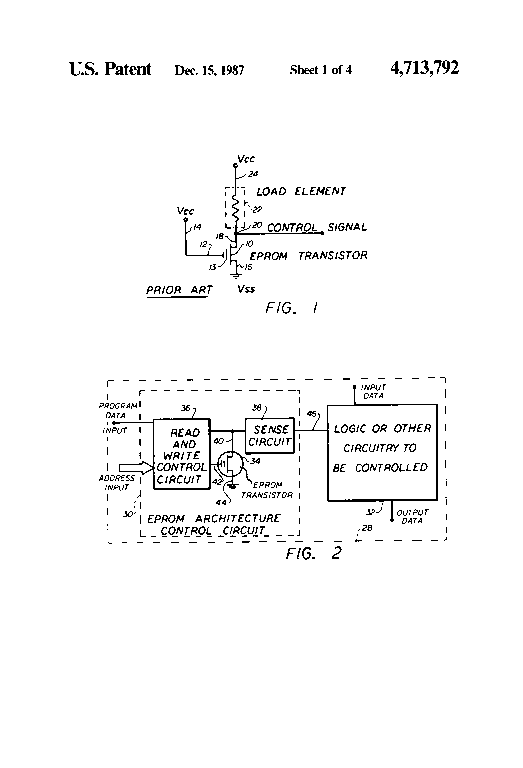
Architecture Feature Programming--The architecture of the EP300 is determined by which paths are selected in the Output and Feedback Multiplexers of FIGS. 14 and 15. These multiplexers are in turn controlled by the Architecture Control Circuits (there is one for each multiplexer control) shown in FIG. 24. The Architecture Control Circuit output consists of an EPROM transistor 200 whose state is "read" by a Schmidt trigger circuit 202. The output of the Schmidt trigger feeds a control gate 204 and the output of the control gate drives the particular multiplexer. There are seven control signals (4 output multiplexer controls and 3 feedback multiplexer controls) per output macro cell requiring 7 Architectural Control Circuits per macro cell. There are eight macro cells thus requiring 56 Architecture control Circuits in the EP300.
The EPROM bits for Architecture Control are programmed as follows. (Refer to FIG. 24). In the Program Mode, NORMOP is at logic 0 turning OFF transistor N2 thus isolating the EPROM bit from FMUX. EPROM transistor 200 is programmed by raising ARDTCNTL at the gate of N1 to VPP. Also, the gate of 200 (PAD-FEED) is raised to VPP by the Architectural Program Decoder (FIG. 20) and a VPP level shifting circuit similar to the Pass Gate Driver (FIG. 22A). At the same time, line 14H10 is raised to a VPP-VT level by a column driver circuit similar to that shown in FIG. 21.
Referring now again to FIG. 24, to verify that the EPROM bit has been programmed, PADFEED and ARDTCNTL are taken to Vcc levels. The Architecture Control Program Driver is then disabled and a sense amplifier is connected to 14H10. The sense amplifier senses the state of the EPROM bit and passes the information to the associated Output Driver.
During the READ Mode, the following conditions apply. ARDTCNTL is taken to Vss thus disconnecting node 7 from line 14H10. PADFEED and NORMOP are taken to Vcc. The state of the EPROM bit can then be determined as follows: first, assume that the EPROM transistor 200 has been programmed. Transistor P1 will then pull node 7 and node 8 to Vcc. This will cause transistors N1 and N2 to turn ON pulling node 12 to Vss. During READ, PRELDBAR is at a logic 1. Thus, with node 12 at logic 0, IOFB will be at logic 1 which selects the I/O Pad as the signal to be passed through FMUX to the Feedback Row Driver. If the EPROM transsitor had been in its erased state, nodes 7 and 8 would have been pulled high. This would force IOFB to a logic 0. Thus, in the Architecture Feature Select, a programmed EPROM bit selects a feature and an unprogrammed bit de-selects a feature. Initially, in the erased state, all features are de-selected.
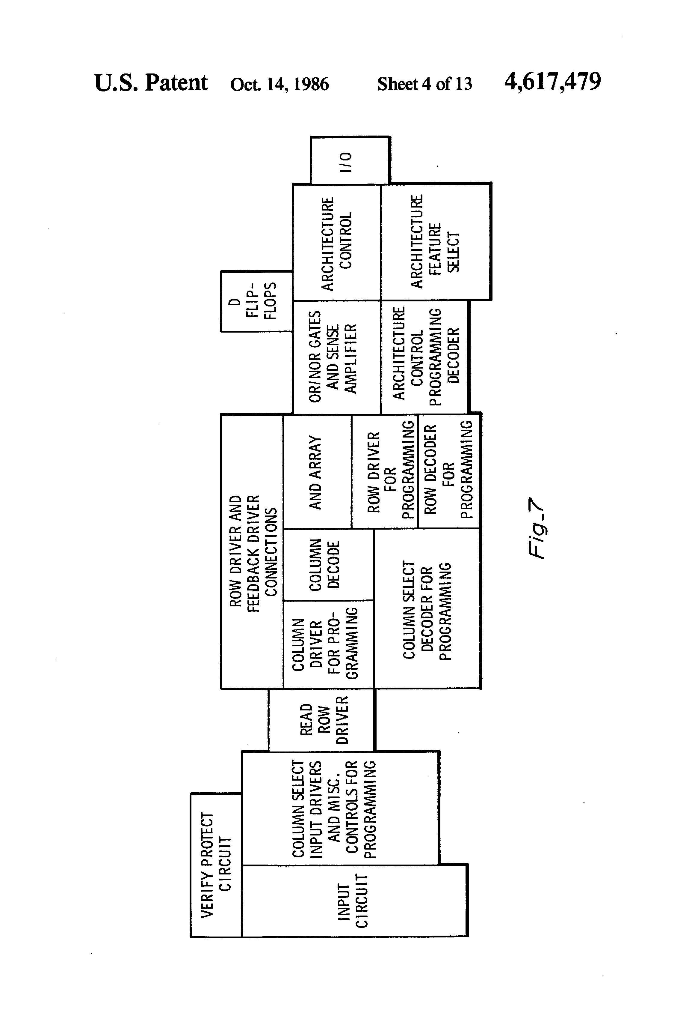
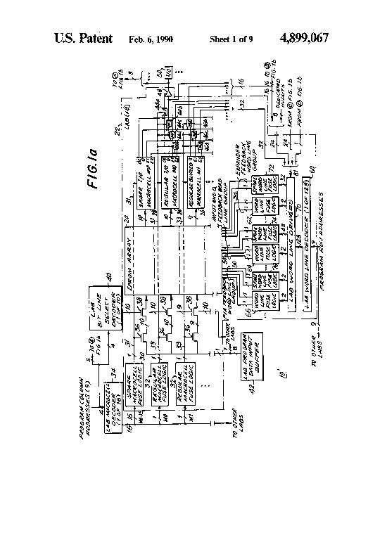
Referring now again to FIG. 17 which is a block diagram of the EP300 for either the Program or the Verify Mode and also referring to the EP300 Mode Select Table for the conditions which select the Verify Mode, it will be seen that the Verify Mode provides a means of interrogating the AND matrix and the Architecture Feature Select Matrix to determine which EPROM transistors have been programmed. Verify Mode is invoked by taking pin 1 to Vhh. All other inputs are then directed through the INPUT CIRCUITS and approximate control circuits to the ROW DECODER, the COLUMN SELECT DECODER and the ARCHITECTURE CONTROL PROGRAM DECODER. Depending upon the state of the inputs, either eight locations in the AND ARRAY or one of the ARCHITECTURE FEATURES associated with each ARCHITECTURE CONTROL block will be directed through the I/O DRIVERS.
Verify is essentially the reverse process from Programming. The location to be interrogated during Verify is determined by the Input Signal exactly as it would be during Programming. The COLUMN DRIVERS and the ARCHITECTURE CONTROL PROGRAM DRIVERS are disabled and corresponding SENSE AMPLIFIERS are enabled. The data which is read by the SENSE AMPLIFIERS is directed to the output pins through the I/O DRIVERS.