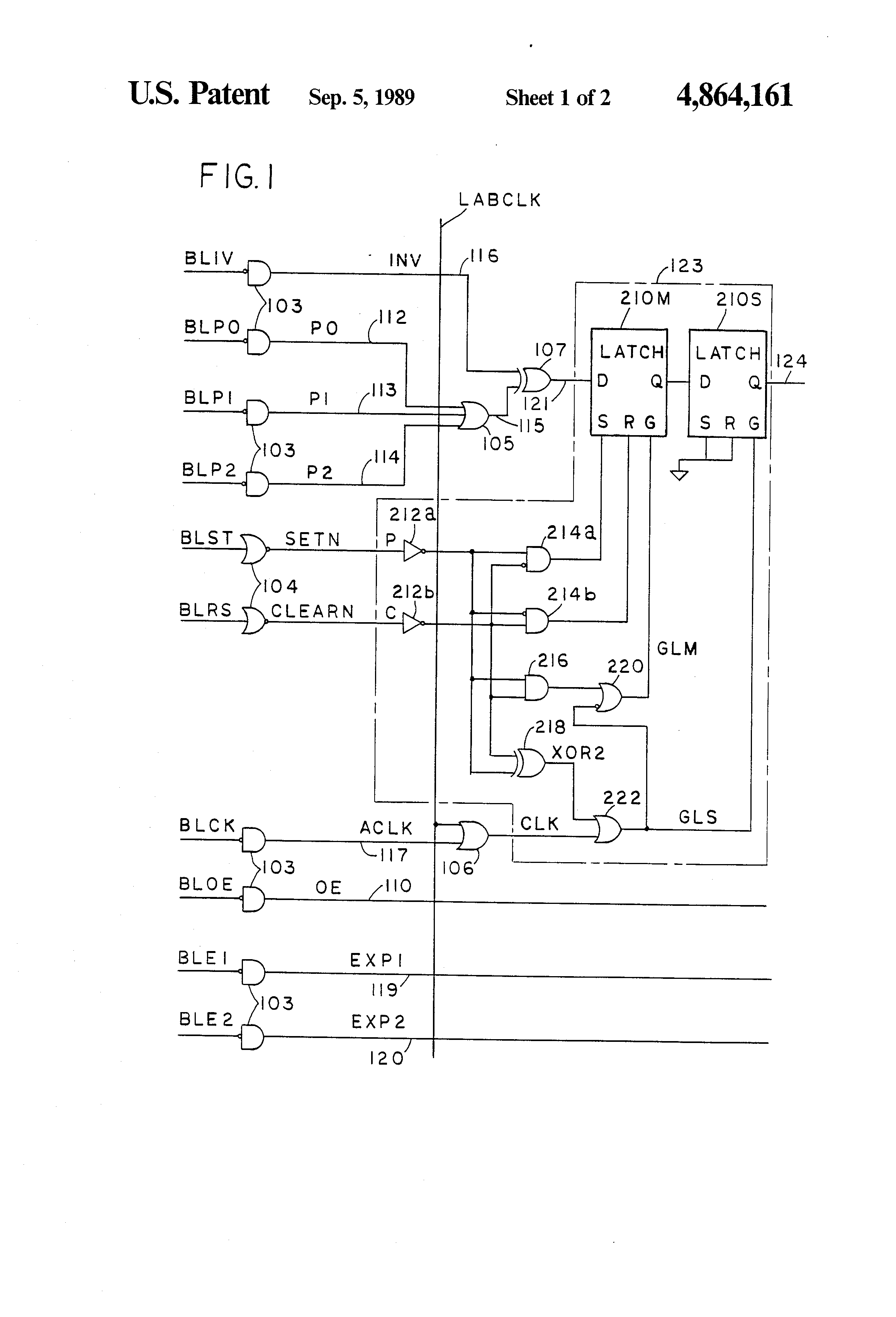
FIG. 1 shows part of the circuitry shown in FIG. 5 of application Ser. No. 190,663. (FIG. 1 is also similar to a portion of FIG. 4 in Ser. No. 190,571, but for convenience herein, only FIG. 5 of Ser. No. 190,663 is referred to below.) Similar names and reference numbers are used for similar elements in these two drawings, although the pictorial arrangement of the elements differs sightly from one drawing to the other. The elements surrounded by chain-dotted line 123 herein correspond to flip-flop 123 in Ser. No. 190,663. (Inverters 212 correspond to the active-low inputs shown on the P and C terminals of flip-flop 123 in that application.)
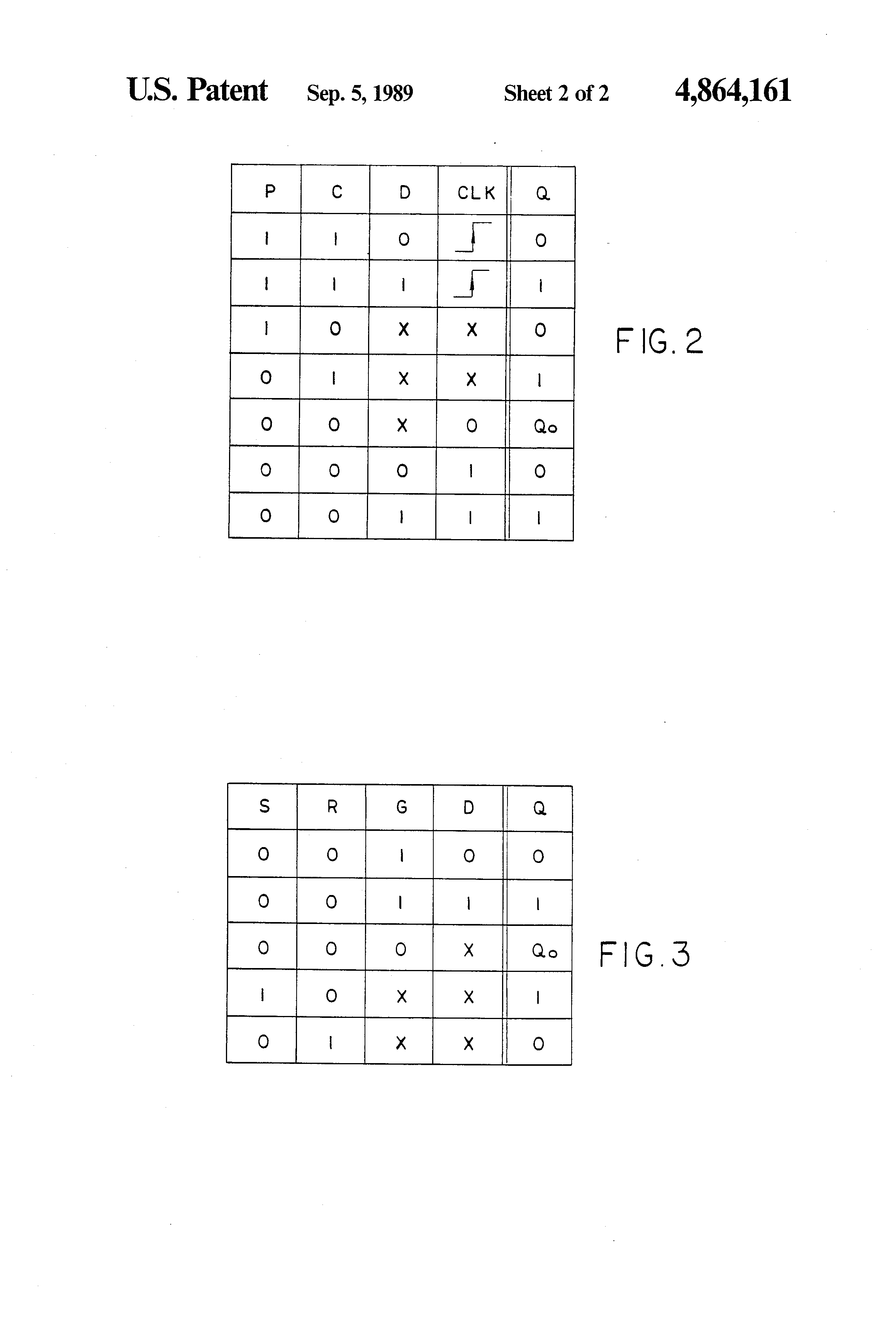
FIG. 2 is a truth table for the overall operation of flip-flop 123. (FIG. 2 corresponds to FIG. 9 in Ser. No. 190,663 and to FIG. 8 in Ser. No. 190,571.) The first four lines of FIG. 2 show that when one or both of the preset P and clear C signals is 1, flip-flop 123 operates like a normal D flip-flop. The last three lines of FIG. 2 show that when P and C are both O (which is normally an illegal condition for a D flip-flop with active-low inputs), flip-flop 123 acts like a flow-through devicce (i.e., Q=D, assuming that the clock signal CLK remains high as shown in the last two lines of FIG. 2), but that (as shown in the third from the last line in FIG. 9) the flow-through data can also be latched into flip-flop 123 by causing CLK to go low (because Qo indicates that Q then holds whatever value it had just before CLK went low). In other words, in addition to being capable of operating as a D flip-flop (first four lines of FIG. 2) or as a flow-through device (last two lines of FIG. 2), flip-flop 123 can also act as a level-sensitive latch by latching in the flow-through data when CLK goes low (third from last line of FIG. 2). FIG. 1 shows the detailed construction of device 123 in accordance with the principles of this invention in order to realize the above-described modes of operation.
Each of latches 210M and 210S is a conventional D latch. Latch 210M is the so-called "master" latch, while latch 210S is the so-called "slave" latch. Each of latches 210 has a data input terminal D, an output terminal Q, a set input terminal S, a reset input terminal R, and a gate or "function enable" input terminal G. FIG. 3 is a truth table for the operation of each of latches 210. As shown in that FIG., when both the set S and reset R inputs of a latch 210 are O and the gate G input is 1, then the Q output follows the data D input. However, when all of S, R, and G are O, the Q output holds whatever value (denoted Qo) it had just before G went low. In other words, with S and R both O, Q is insensitive to changes in D while G is low. When S is 1 and R is O, Q is 1 regardless of G and D. Similarly, when S is O and R is 1, Q is O regardless of G and D. In the ensuing discussion, an M or S suffix is sometimes used to distinguish the signals associated with master latch 210M from the signals associated with slave latch 210S. For example, DM refers to the D signal of master latch 210M, while DS refers to the D signal of slave latch 210S.
The P and C signals (corresponding respectively to the P and C signals in Ser. No. 190,663 ) and to the PRE and CLR signals in Ser. No. 190,571) are respectively inverted by inverters 212a and 212b and then applied to one input of each of AND gates 214a and 214b. The inverse of the inverted C signal is applied to the other input of AND gate 214a, and the inverse of the inverted P signal is applied to the other input of AND gate 214b. The effect of AND gates 214 is to make it impossible for both SM and RM to be 1 at the same time. Assuming, however, that no more than one of P and C is 0, gates 214 effectively apply the inverted P signal to the S terminal of latch 210M, and the inverted C signal to the R terminal of latch 210M. Accordingly, if either P or C is 0 QM is determined by which of P and C is 0. QM is then passed through to QS because with either P or C 0, the output XOR2 of EXCLUSIVE OR ("XOR") gate 218 becomes 1 and the output GLS of OR gate 222 also becomes 1. (SS and RS are always tied low.) The above-described operation corresponds to the third and fourth lines of FIG. 2.
If both P and C are 1, SM and RM are both O. The output of AND gate 216 is O, and so is the output of XOR gate 218. OR gate 222 then passes whatever CLK signal is applied to it, and that signal is inverted by OR gate 220. Assuming that the CLK signal is initially low, GM is high and DM is passed to QM and thereby applied to DS. When the CLK signal subsequently goes high, DS is passed to QS. This mode of operation corresponds to the first two lines of FIG. 2.
If P and C are both 0, SM and SR are also both O. The output of AND gate 216 is 1, the output of OR gate 220 is 1, and the output of XOR gate 218 is O. If CLK is also 1 (e.g., because BLCK is tied low), the output of OR gate 106 is 1, and the output of OR gate 222 is also 1. This means that each of latches 210 operates as shown in the first two lines of FIG. 3 so that QS=DM. In other words, whatever data is applied to DM flows through to QS. This mode of operation corresponds to the last two lines of FIG. 2.
If, at any time during the flow-through operation described immediately above, CLK goes low (e.g., because BLCK is not in fact permanently tied low), the output of OR gate 222 becomes O. This causes latch 210S to operate as shown in the third line in FIG. 3, thereby latching in the current value Qo of QS. This mode of operation corresponds to the fifth line of FIG. 2.
From the foregoing, it will be apparent that the circuit of FIG. 3 can be used to supply on lead 124 either the "registered" or "combinatorial" output of XOR gate 107 (registered output results from operation of device 123 as a D flip-flop (first four lines of FIG. 2); combinatorial output results from operation of device 123 in the flow-through mode (last two lines of FIG. 2)), and that in addition, the flow-through mode data can be latched into device 123 at any time by causing the CLK signal to go low. Device 123 is therefore highly flexible and of great utility in programmable logic device ("PLDs") such as are shown in Ser. Nos. 190,663 and 190,571.
Although particular signal values like "0" and "1" or "first polarity" and "second polarity" are referred to herein and in the appended claims, it will be understood that these values and terms are purely arbitrary, and that they are used solely for purposes of illustration. Thus, for example, although "first polarity" is uniformly equated with logic 0, and "second polarity" is uniformly equated with logic 1 herein as an aid to understanding the specification and claims, this is not necessarily the case, and the polarity or value of various signals can be reversed or otherwise altered without departing from the scope and spirit of the invention. As another example, whereas the specification and claims sometimes refer to applying the inverse of a particular signal to a particular component, if the polarity of that signal were reversed, then the signal could be applied directly (without inversion) to that component. Again, such polarity reversals and the consequent elimination (or addition) of inversions is entirely within the scope of the invention.