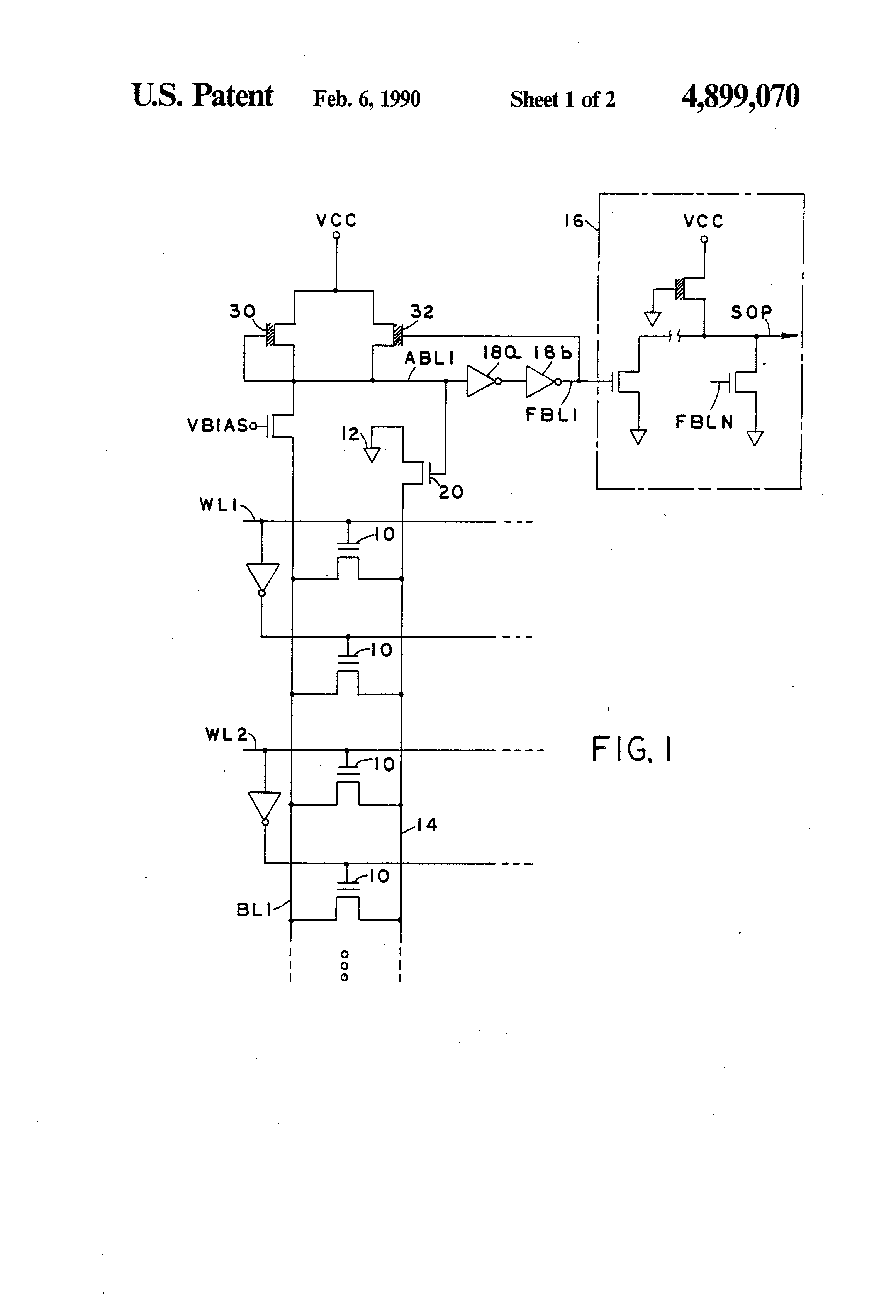
FIG. 1 shows part of the conventional circuitry for a PLD which has been modified in accordance with the principles of this invention. EPROMs 10 are programmable interconnections between each of a plurality of input word lines WL1, WL2, etc., and each of a plurality of bit lines BL1, BL2, etc. (only one of which is shown in FIG. 1). As is usual (although not always necessary), both the true and complement versions of each word line signal are connectable to each bit line.
EPROMs 10 are individually programmed in advance so that each EPROM either does or does not apply the associated work line signal (true or complement) to the associated bit line. For example if a particular EPROM 10 is programmed to apply associated (true or complement) word line signal to the associated, bit line, then when that (true or complement) word line signal is logic 1, the EPROM connects the bit line to "ground" (logic 0) at point 12 via the "virtual" ground line 14 and current limiting device 20 associated with that bit line. This causes the bit line to go low (logic 0), which in turn causes the amplified bit line signal (e.g., ABL1) and the final bit line signal (e.g., FBL1) to also go low. Typically (although not necessarily) several final bit line signals are combined in additional logic circuitry 16 to provide a sum-of-products output signal SOP which may be either output from the PLD or further processed in the PLD.
Typical voltages in the circuit are as follows: VCC is 5 volts; VBIAs is approximately 2.5 volts; ground (e.g., point 12) is 0 volts; logic 0 on BL1 is typically less than 1 volt; logic 1 on BL1 is typically greater than 1 volt; logic 0 on ABL1 is approximately 1.2 volts; logic 1 on ABL1 is 3 to 3.5 volts; logic 0 on FBL1 is approximately 0 volts; and logic 1 on FBL1 is approximately 5 volts. Thus inverters 18a and 18b collectively comprise a circuit for sensing the potential difference between the logical states of the ABL1 signal and for amplifying that signal to the normal CMOS (complementary metal oxide semiconductor) levels of 0 and 5 volts. It will be understood that the particular voltages mentioned above are merely illustrative, and that they are provided solely as an aid to understanding the depicted circuit. Those skilled in the art will appreciate that any or all of these voltages can be altered, even to the point of reversing polarities, without departing from the scope and spirit of the invention. For example, although "ground potential" is referred to herein and in the appended claims, it will be understood that this is merely an arbitrary term and that it is not used in any absolute sense. Thus the potential referred to as "ground potential" could be any potential different from (i.e., higher or lower than) VCC.
Although only a small number of word lines are shown connectable to bit line BL1 in FIG. 1, it is not at all unusual in current PLD designs for there to be 100 or more word lines connectable to each bit line. Similarly, although one one bit line BL1 is shown in FIG. 1, it is not at all unusual for there to be 100 or more bit lines connectable to each word line.
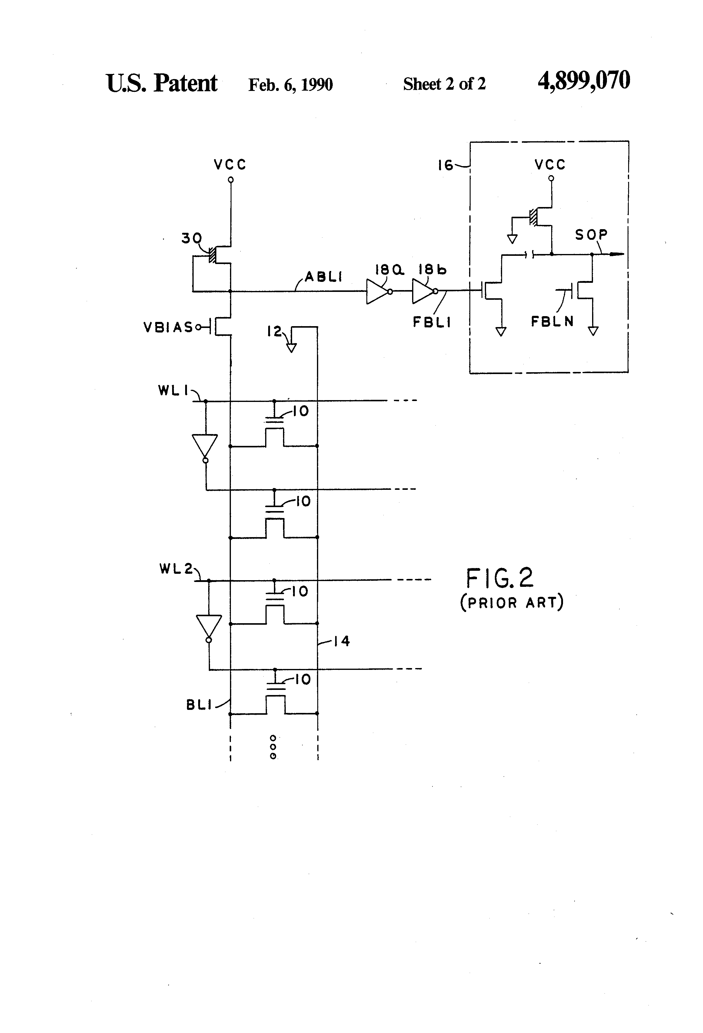
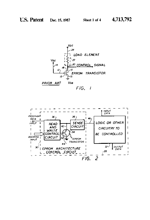
When only a relatively small number of the EPROMs connected to bit line BL1 are turned on, the voltage on BL1, although logic 0, may remain relatively high (e.g., typically less than but relatively close to 1 volt). Thereafter, when all of these EPROMs are turned off, the voltage on BL1 can be pulled up to logic 1 relatively quickly. However, when a relatively large number of the EPROMs connected to bit line BL1 are turned on in the absence of this invention (as in the case of the prior art circuit shown in FIG. 2), the voltage on BL1 tends to go very close to ground (e.g., very close to 0 volts). This means that it takes substantially longer to pull the voltage on BL1 up to logic 1 when all of the EPROMs turn off. This data pattern is normally the "worst case" for the transition of BL1 from logic 0 to logic 1.
In accordance with the present invention as shown in FIG. 1, current limiting transistor 20 is connected in series between the virtual ground line 14 associated with bit line BL1 and the actual source 12 of ground potential. (In the depicted embodiment, transistor 20 is an n-channel transistor which is off when its gate is low.) The gate of transistor 20 is connected to ABL1. Because the voltage of ABL1 is designed to be always higher than the threshold voltage of an n-channel transistor, transistor 20 is therefore on at all times. However, as the voltage on BL1 comes closer to ground and therefore the voltage on ABL1 also falls correspondingly, transistor 20 becomes less conducting. This prevents the voltage on BL1 from dropping excessively low even when large numbers of EPROMs 10 are conducting. THis in turn improves the switching speed of the device when all of EPROMs 10 turn off because the voltage on BL1 does not have to be pulled up so far to reach the threshold for logic 1.
Another aspect of the invention involves the provision of two transistors 30 and 32 connected in parallel with one another between reference potential source VCC and ABL1. (In the depicted embodiment, each of transistors 30 and 32 is a p-channel transistor which is off when its gate is high.) The gate of transistor 30 is connected to ABL1, while the gate of transistor 32 is connected to FBL1. Transistor 30 is preferably a relatively small device which is on at all times providing a relatively small "leakage" current from VCC to ABL1. Ideally, the logic 1 state of ABL1 should be biased close to the trip-point of the subsequent inverter stage 18a. In this embodiment, the logic 1 state of ABL1 is limited to VCC minus Vtp (where Vtp is the threshold voltage of p-channel transistor 30). Transistor 32, on the other hand, is preferably a relatively large device which is on only when ABL1 is logic 0. Thus when all of EPROMs 10 turn off, the relatively large current flowing through transistor 32 is available to help rapidly pull up ABL1 from logic 0 to logic 1. On the other hand, as soon as ABL1 reaches logic 1, transistor 32 shuts off so that it does not retard a subsequent transition from logic 1 to logic 0.
The difference in voltage on ABL1 between the logic states and the trip point of inverter state 18a determines the noise immunity of the sense amplifier stage. In this embodiment, inverter 18a is designed with its trip point at about one-half VCC or 2.5 volts. For logic 1, the noise margin is therefore calculated to be 0.5 VCC minus Vtp. For logic 0, ABL1's voltage is determined by the ratio of the combined currents through pull- up transistors 30 and 32 versus the current through the EPROM cell 10 and current limiting device 20. As mentioned above, the logic 0 state of ABL1 is about 1.2 volts. Therefore, the noise margin for logic 0 is calculated to be 0.5 VCC minus 1.2 volts. Because Vtp is typically about 1 volt, the noise margins for both logic states are similar.
It will be understood that the foregoing is merely illustrative of the principles of this invention, and that various modifications can be made by those skilled in the art without departing from the scope and spirit of the invention. For example, although particualr voltage values and device types (e.g., n-channel or p-channel transistors) have been mentioned, it will be understood that other voltages and devices can be used if desired. Thus transistor 30 could be an n-channel transistor with its gate tied to VCC. With this configuration, the logic state of ABL1 is limited to VCC minus Vtn (where Vtn is the threshold voltage of n-channel transistor 30).