In accordance with an aspect of the invention, an analog or multilevel memory includes multiple arrays of memory cells where each memory array has local row lines, local column lines, and/or local source lines coupled to local decoders. Local row, column, and source lines of the different arrays are electrically separated to reduce the number of memory cells in the same row or column as memory cells being program and reduce the number of threshold voltage disturbances. Accordingly, the multiple array architecture reduces the accumulated threshold voltage disturb when compared to a memory architecture having a single larger array. In accordance with a further aspect of the invention, the memory includes global decoders such as a global row decoder and/or a global column decoder with global row lines and/or global column lines for multiple arrays. The local column or row decoders connect the global column or row lines to the local column or row lines of a selected array containing a memory cell being programmed. The combination of global and local decoding reduces the complexity and the total decoding circuitry required for the memory.
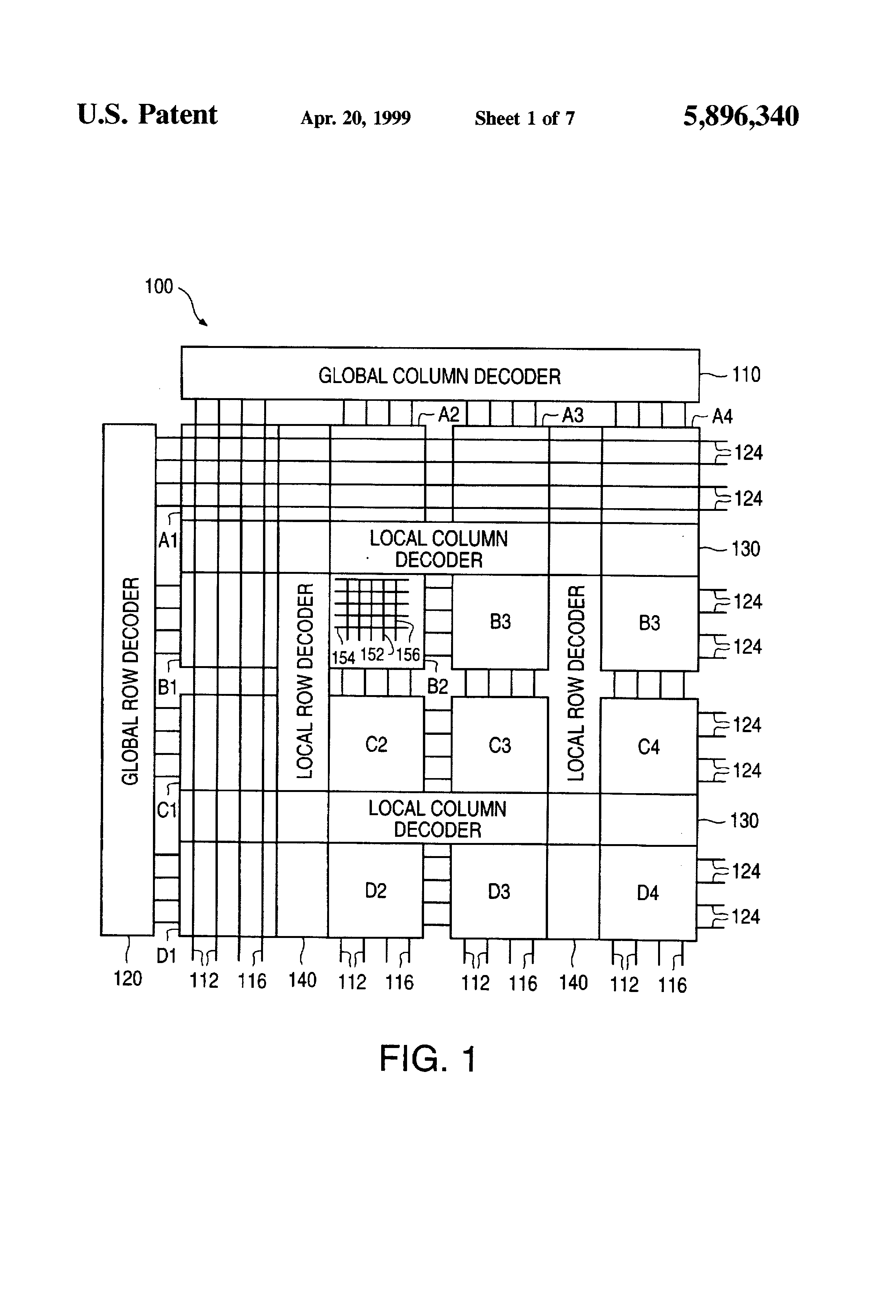
FIG. 1 shows a memory 100 in accordance with an embodiment of the invention. Memory 100 is an integrated circuit formed on a single semiconductor substrate including sixteen arrays A1 to D4 of memory cells which are arranged in four columns A1 . . . D1, A2 . . . D2, A3 . . . D3, and A4 . . . D4 of arrays and four rows A1 . . . A4, B1 . . . B4, C1 . . . C4, and D1 . . . D4 of arrays. Alternative memory architectures in accordance with the invention can include any integer number x of columns of arrays and any integer number y of rows of arrays where x or y is greater than 1. Memory 100 illustrates an example where x and y are equal to 4. Each of memory arrays A1 to D4 contains i columns and j rows of memory cells coupled to i local column lines 152 and j local row lines 154. For ease of illustration, FIG. 1 only shows local column lines 152 and local row lines 154 in array B2, but each of arrays A1 to D4 has similar local row and column lines. Each row or column of memory array 100 includes four electrically separated local rows or columns in four different arrays. In an exemplary embodiment, memory 100 is a flash memory, and each of arrays A1 to D4 has one or more local source lines 156, where each source line 156 corresponds to an independently erasable sector in the array. The local column, row, and source lines in each array are electrically isolated from the local column, row, and source lines of the other arrays.
Arrays A1 to D4 may be constructed using known memory array architectures. In the exemplary embodiment, each array of memory cells A1 to D4 is an array of n-channel floating gate transistors. Each n-channel floating gate transistor has source, drain, and channel regions disposed in a semiconductor substrate, a floating gate overlying the channel region, and a control gate overlying the floating gate. Insulating layers between the substrate and the floating gates and between the floating gates and the control gates isolate the floating gates from direct electrical contact, but channel hot electron injection or Fowler-Nordhiem tunneling through the insulating layers can charge or discharge the floating gate and change the threshold voltage of the memory cell during a program or erase operation. In the exemplary embodiment, drain and source regions are diffused in a silicon substrate. Floating gates are formed in a first polysilicon layer overlying the substrate. Local row lines 154, each of which forms the control gates of the floating gate transistors of a local row, are formed in a second polysilicon or silicide layer. Local column lines 152 and local source lines 156 are formed in a first metal layer and contact underlying diffused regions in the substrate. In particular, the source regions of the floating gate transistors in a sector of the exemplary memory array are portions of diffused local source lines (not shown) in the substrate, and each local source line 156 straps together the diffused local source lines for a sector. In the exemplary embodiment, each erasable sector contains multiple local columns of memory cells (i.e., is column based), and the diffused local source lines connect multiple memory cells from the same or adjacent rows. Alternative embodiments may have row-based sectors (each sector containing one or more local rows) and/or use other semiconductor memory structures.
Overlying arrays A1 to D4 are continuous global column lines 112, global row lines 124, and global source lines 116 which in the exemplary embodiment are formed from second and third metal layers. Global column, row, and source lines 112, 124, and 116 connect global decoders 110 and 120 to local decoders 130 and 140. Generally, memory 100 contains n global column lines 112 and m global row lines 114 where n is less than or equal to the number x*i of columns in memory 100 and m is less than or equal to the number y*j of rows in memory 100, x, y, i, and j being defined above. The exemplary embodiment has twices as many columns as global column lines (x*i=2n.) Local decoders 130 and 140 between arrays A1 to D4 select an array or arrays and connect global column, row, and source lines 112, 124, and 116 to selected local column, row, and source lines 152, 154, and 156 in the selected array or arrays.
To access a selected memory cell in one of arrays A1 to D4, column decoder 110 decodes bits from a column address signal to select a global column line 112 corresponding to a column of memory cells containing the selected memory cell. Drivers in global column decoder 110 apply voltages to the selected global column and source lines 112 and 116 as required for the access to the selected memory cell. Local column decoders 130 decode bits from a row address signal to select a row or bank of arrays A1 . . . A4, B1 . . . B4, C1 . . . C4, or D1 . . . D4 that contains the selected memory cell and connects global column lines 112 to local column lines 152 in the selected arrays. If, for example, the number n of global column lines 112 is equal to the total number (x*i) of columns in memory 100, global column lines 112 have a one-to-one correspondence with local column lines 152 in the selected row of arrays, and local column decoders 130 connect each global column lines 112 to the corresponding local column line in the selected row of arrays. If there are fewer global column lines 112 than local column lines 152 in a row of arrays, then at least some global column lines 112 correspond to more than one local column line 152 in the selected row of arrays; and for each global column line 112, local column decoders 130 select which of the local column lines corresponding to the global column line is connected to the global column line. Local decoders 130 decode bits of the column address to select from among multiple local column lines corresponding to a single global column line. Additionally, in the exemplary embodiment where erase sectors are column-based, global column decoder 110 controls voltages on global source lines 116 which are intermixed with global column lines 112, and local decoders 130 connect global source lines 116 to local source lines 156 in the selected row of arrays.
Global row decoder 120 decodes bits from the row address signal to select a global row line 124 that corresponds to the selected memory cell and applies to the selected global row line 124 a voltage required to access the selected memory cell. Local decoders 140 decode bits from the column address signal to select a column or bank of arrays A1 . . . D1, A2 . . . D2, A3 . . . D3, or A4 . . . D4 that contains the selected memory cell to be accessed and connects global row lines 124 to local row lines 154 in the selected column of arrays. For embodiments where global row lines 124 are in one-to-one correspondence with the local row lines 154 in a column of arrays (i.e., for m=y*j), local decoders 140 connect each local row line 154 in the selected column of arrays to its corresponding global word line 124. Alternatively, where each array A1 to D4 contains more than one local row line 154 that corresponds to the same global row line 124, local decoders 140 additionally decode bits from the row address to select which local row line is connected to the corresponding global row line.
Memory 100 reduces program disturb by only applying programming voltages to the one of arrays A1 to D4 that contains a selected memory cell being programmed. For example, channel hot electron injection programs an n-channel memory cell by charging the floating gate and increasing the threshold voltage of the memory cell. For channel hot electron injection, a relatively large voltage difference is created between the control gate and the source of a memory cell while the memory cell conducts a source-drain current. Programming voltages Vrp and Vcp of about 10 volts and 6 volts respectively applied to the control gate and drain of a typical flash memory cell while the source of the memory cell is grounded will cause channel hot electron injection that raises the threshold voltage of the memory cell. Alternatively, the programming voltage Vrp may depend on an analog value being written and range between 8 and 11 volts. Programming voltages Vrp or Vcp when applied to unselected memory cells in the same local row or column as the selected memory cell can cause tunneling which disturbs the threshold voltage of the unselected memory cells. In memory 100, row decoder 120 applies programming voltage Vrp to a single selected global row line 124, and local decoders 140 only apply programming voltage Vrp from the selected global row line 124 to a single local row line 154. Column decoder 110 applies programming voltage Vcp to a single selected global column line 112, and local decoders 130 only apply programming voltage Vcp from the selected global column line 112 to a single local column line 154. Thus, the only unselected memory cells disturbed are in the selected one of arrays A1 to D4.
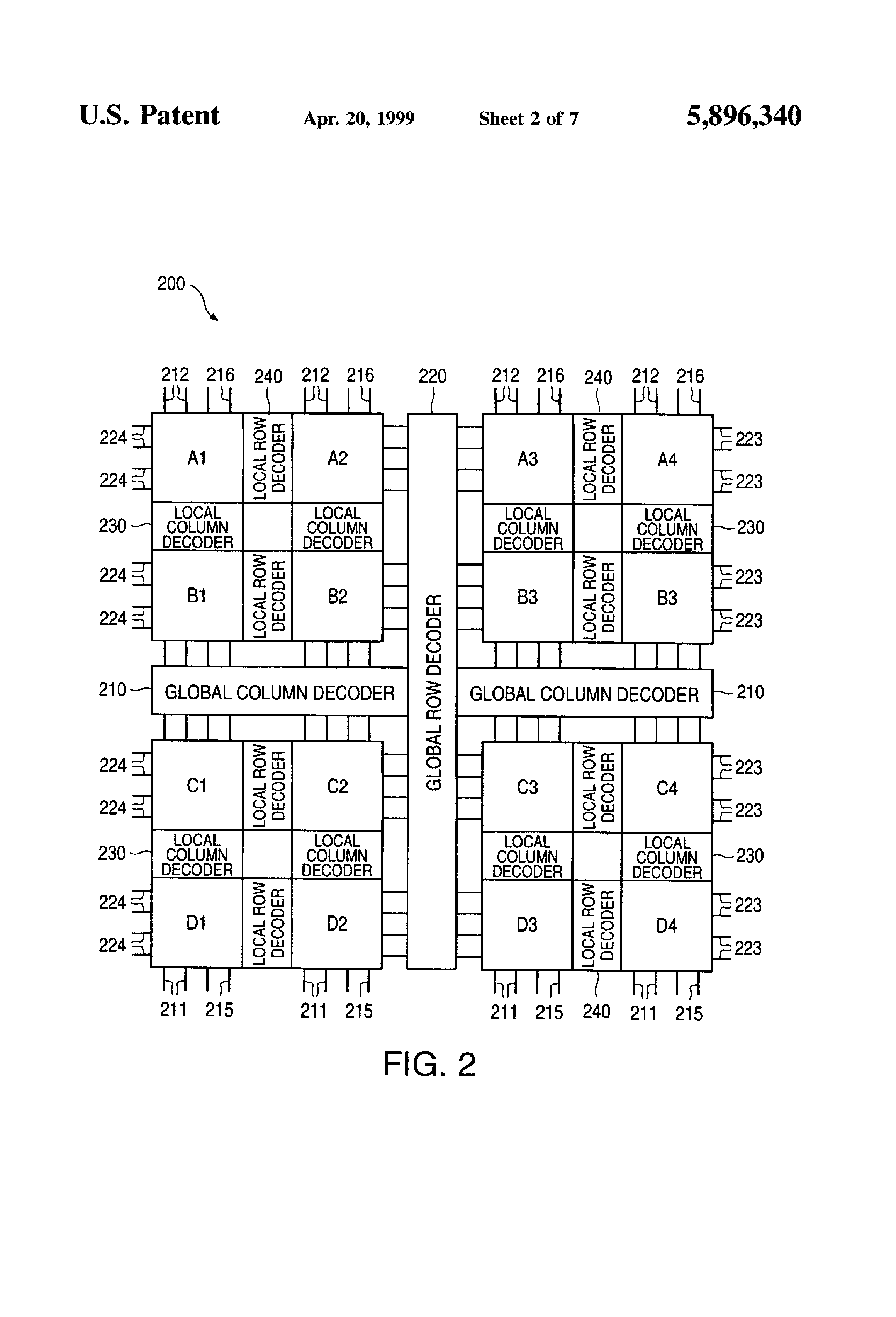
FIG. 2 shows a memory 200 having a global column decoder 210 and a global row decoder 220 between arrays of memory arrays. Global column lines 212 and 211 respectively extend upward and downward from global column decoder 210. As in the memory 100 of FIG. 1, arrays A1 to D4 have column based erase sectors, and global source lines 216 and 215 for the erase sectors respectively extend upward and downward from global column decoder 210. Global row lines 224 and 223 respectively extend left and right of global row decoder 220. Each global column, source, or row line 211, 212, 215, 216, 223, or 224 is continuous and coupled to local column decoders 230 or local row decoders 240. Local column decoders 230 select which row of arrays A1 . . . A4, B1 . . . B4, C1 . . . C4, or D1 . . . D4 are connected to global column lines 211 or 212 or source lines 215 or 216. Local row decoders 140 select which column of arrays A1 . . . D1, A2 . . . D2, A3 . . . D3, or A4 . . . D4 are connected to global row lines 223 or 224.
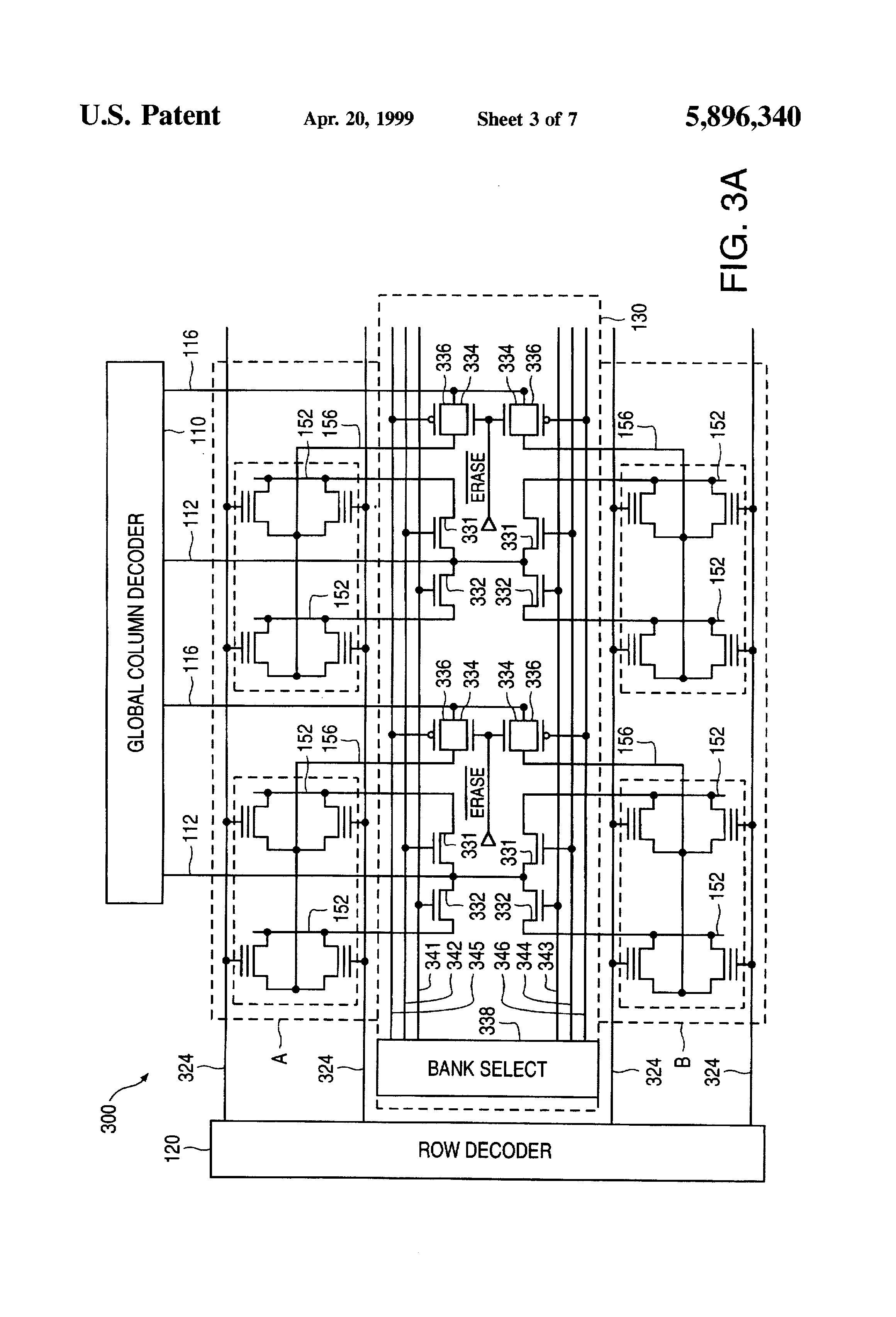
FIG. 3A shows a memory 300 having two memory arrays A and B arranged in a column. (In memory 300, the number x of column/banks of memory arrays is 1, and the number y of row/banks of memory arrays is 2.) Memory 300 can be expanded to include a single column of more than two memory arrays with additional local decoders between pairs of memory arrays. For ease of illustration, each of memory arrays A and B contains two rows of memory cells connected to row lines 324 and four columns of memory cells coupled to local column lines 152. In an actual memory, each of arrays A and B would contain hundreds of rows and columns of memory cells, the size of each memory array being selected according to the memory cell technology and an acceptable amount of threshold voltage disturb. Since memory 300 only contains one column of memory arrays, row lines 324 are both local row lines for arrays A and B and global row lines for memory 300. This reduces the number of metal layers required when forming memory 300 because row lines 324 are formed from the control gate layer and an overlying metal for global row lines is not required.
Row decoder 120 is a conventional row decoder that decodes a row address to select a row line 324 coupled to a selected memory cell and applies to the selected row line a voltage required for accessing the selected memory cell. Column decoder 110 decodes a column address to select the global column line 112 corresponding to the selected memory cell and applies to the selected column line a voltage required for accessing the selected memory cell. In memory 300, each array A or B includes two local column lines 152 for each global column line 112. Accordingly, a column address identifying the selected memory cell includes a set of bits (for example, the most significant column address bits) that identifies the selected global column line and a set of bits (for example, the least significant column address bits or bit) that identifies one of the local column lines corresponding to the selected global column line. Global column decoder 110 decodes the set of column bits identifying the selected global column line. Local decoder 130 decodes the set of column address bits that select among the local column lines corresponding to each global column line. Local decoder 130 also decodes a set of the row address bits to identify which array A or B contains the selected cell.
Global column decoder 110 also controls the voltages on global source lines 116. In the exemplary embodiment of the invention, all of global source lines 116 are grounded except during an erase. When erasing a selected sector in a select one of arrays A and B, global column decoder 110 applies an erase voltage Vse (typically about 12 volts) to the one of global source lines 116 corresponding to the selected sector and grounds the remaining global source lines 116. Local decoder 130 selects the row of arrays (e.g., array A or array B) containing the sector to be erased and connects local source lines 156 in the select row/bank of arrays to global source lines 116.
Local column decoder 130 includes transistors 331 and 332 coupled between global column lines 112 and corresponding local column lines 152 and transistors 336 coupled between global source lines 116 and corresponding local source lines 156. A bank select circuit 338 decodes address signals to turn on selected ones of transistors 331, 332 and 336. In particular, for a read or write, bank select circuit 338 decodes the most significant bit of the row address of a selected memory cell to determine which array A or B contains the selected memory cell and decodes the least significant bit of the column address to determine whether the selected memory cell is in an even or odd number column of memory 300. Transistors 332 for the selected array A or B are turned on if the column address is even, and transistors 331 for the selected array A or B are turned on if the column address is odd. To turn on the desired ones of transistor 331 and 332, bank select circuit 338 asserts a signal on a line 341 if the selected memory cell is in an even column of array A, asserts a signal on a line 342 if the selected memory cell is in an odd column of array A, asserts a signal on a line 343 if the selected memory cell is in an even column of array B, and asserts a signal on a line 344 if the selected memory cell is in an odd column of array B. In alternative embodiments, more than two local column lines 152 can correspond to the same global column line 112. The number of local columns of memory cells corresponding to a global column line may be selected according to pitch of the memory cells in the arrays and the available area for local decoding circuits between the arrays.
Transistors 336 are off and transistors 334 ground all local source lines 356 of arrays A and B to global source lines 316 except during an erase. During an erase, all of transistors 331, 332, and 334 are off, and bank select circuit 338 asserts a signal on line 345 or 346 to turn on transistors 336 that are coupled to the array A or B containing the sector being erased. The unselected global and local source lines 116 and 156 in array A and B float during an erase.
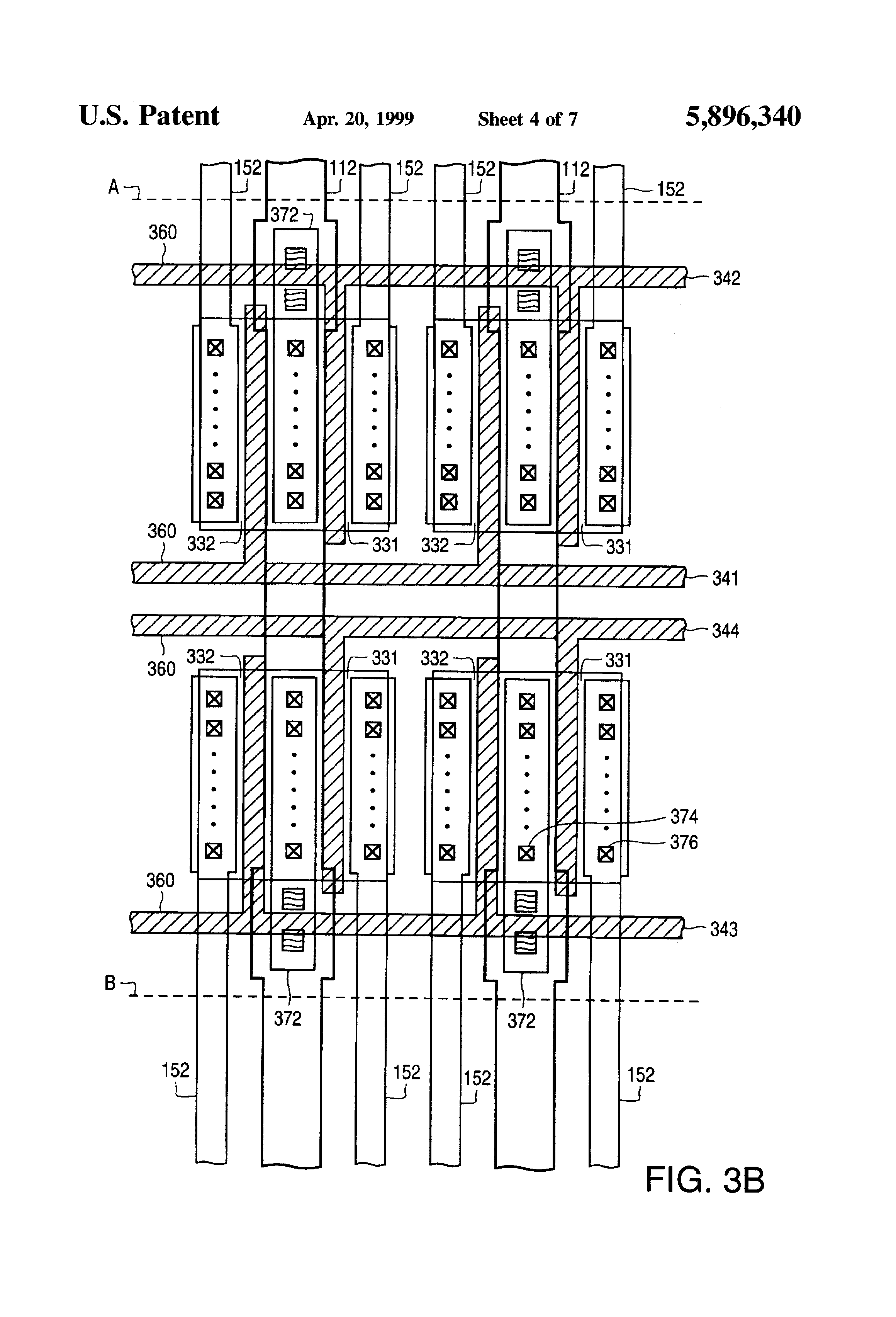
FIG. 3B shows a layout for regions in an integrated circuit forming a portion of memory 300 and local column decoder 130. In particular, FIG. 3A shows transistors 332 and 331 which connent global column lines 112 to local column lines 152 in arrays A and B. Transistors 331 and 332 have gates formed from portions of a low resistance polysilicon regions 360 which also form lines 341 to 344 connecting transistors 331 and 332 to bank select circuit 338. Polysilicon regions 360 may be formed from a first or second polysilicon layer used for floating or control gates in the memory cells. Source/drain regions for transistors 331 and 332 are formed in a substrate underlying polysilicon regions 360 and connected to overlying metal regions. A first metal layer is patterned to form local column lines 152 and interconnects 312. Contacts 376 connect each local column line 152 to a separate source/drain region of an associated transistor 331 or 332. Contacts 374 connect interconnets 372 to source/drain regions shared by adjacent pairs of transistors 331 and 332, and contacts 382 connect global lines 112, which are formed in a second metal layer, to associated interconnects 372.
FIG. 4 shows a memory 400 including two arrays A1 and A2 arranged in a row. FIG. 4 shows each of arrays A1 and A2 as having two rows and two columns of memory cells. In an actual memory, each array would typically have hundreds of rows and columns. Each row of memory cells is coupled to a local row line 154, and each column of memory cells is coupled to a column line 412. Column lines 412 act as both local column lines coupled to the drains of memory cells and global column lines coupled to global column decoder 110. Memory 400 includes global column decoder 110 and global row decoder 120 that during a read or write respectively decode column and row address signals to select a respective column line 412 or global row line 124 corresponding to the memory cell identified by the column or row address.
Local decoder 140 is between the two columns of arrays and includes row line selection transistors (or pass gates) 442 and a bank select circuit 448. Each transistor 442 connects a global row line 124 to a corresponding local row line 154. In memory 500, each global row line 124 corresponds to two local row lines 154 in adjacent row. Alternatively, each global row line 124 corresponds to only one local row line 154 in a column of arrays or more than two local row lines. For a particular memory architecture the number of local row lines per global row line is limited by the pitch of the memory arrays and the available area for local decoding circuitry between arrays. Bank selection circuit 448 decodes a set of bits (e.g., the most significant bit) from the column address of a selected memory cell to select the memory array A1 or A2 containing the selected memory cell and a set of bits (e.g., the least significant bit) from the row address of the selected memory cell to determine for each global row line which of the two corresponding local row lines in the selected array is coupled to the global row line. To turn on the desired ones of row line select transistors 442, bank select circuit 448 asserts a signal on a line 461 if the selected memory cell is in an odd row of array A1, asserts a signal on a line 462 if the selected memory cell is in an even row of array A1, asserts a signal on a line 463 if the selected memory cell is in an even row of array A2, and asserts a signal on a line 464 if the selected memory cell is in an odd row of array A2.
FIG. 5 shows a memory 500 including four arrays A1, A2, B1, and B2 arranged in two rows and two columns. Each of arrays A1 to B2 is illustrated as having two columns of memory cells that are coupled to local column lines 152 and two rows of memory cells that are coupled to local row lines 154. In an actual memory, each array would typically have hundreds of local rows and columns. Memory 500 includes global column decoder 110 and global row decoder 120 that operate as described above. Local column decoder 130, which is between the two rows of arrays, decodes a set of bits of the row address of a selected memory cell to determine which row of arrays array A1, A2 or B1, B2 contains the selected memory cells and connects global column and source lines 112 and 116 to local column and source lines 152 and 156 in the selected row of arrays. Local decoder 130 also decodes the least significant bit of the column address to determine whether the selected memory cell is in an even or odd column of memory 500 and connects the even or odd numbered local column lines to global column lines 112. The circuitry within an embodiment of local decoder 130 is described above in regard to FIG. 3.
Local row decoder 140, which is between the two columns of arrays, decodes a set of bits of the column address of the selected memory cell to determine which column of arrays array A1, B1 or A2,B2 contains the selected memory cells and connects global row lines 124 to local row lines 154 in the selected column of arrays. Local decoder 140 also decodes the least significant bit of the column address to determine whether the selected memory cell is in an even or odd row of memory 500 and connects on the even or odd numbered local row lines 154 to global row lines 124. The circuitry within an embodiment of local decoder 140 is described above in regard to FIG. 4.
Memory 500 can be expanded by adding additionally memory arrays and local decoders, for example, as illustrated in FIGS. 1 and 2.
In above described embodiment, multiple array memory architectures having local decoders that separate global row or column lines from local row or column lines. These architectures reduce threshold voltages disturbances by preventing programming the voltages on the global lines from being applied to the local lines or the memory cell in memory arrays not containing the memory cell being programmed. In an alternative, memory architecture multiple arrays have memory cells directly coupled to continuous global row and column lines so that the row or column programming voltage is applied to unselected cells, but the unselected memory arrays have local source decoders and local source lines that are biased to reduce disturbances that applying the programming voltage to unselected cells causes.
FIG. 6 illustrates a memory 600 having this alternative memory architecture. Memory 600 includes multiple arrays A1 . . . D2, a global column and source decoder 610, a global row decoder 620, and local source decoders 630. Global row decoder 620 is between the two columns of arrays A1 . . . D1 and A2 . . . D2 and is coupled to continuous row lines 624 that are directly coupled to memory cells. Global column decoder 610 is coupled to continuous column lines 612 and global source lines 616. Each column line 612 directly couples to a column of memory cells (i.e., memory cells from multiple arrays), and each global source line 616 couples to local source decoders 630. Each local source line 656 is coupled to memory cells in a sector of one array and isolated from memory cells in other arrays. In an exemplary embodiment, sectors are row based so that each local source line 656 is electrically coupled to multiple local columns of an array. Alternative memory architectures use row-based sectors.
During programming, drivers associated with global row decoder 620 apply the programming voltage Vrp (between 6 and 12 volts for typical analog or multilevel Flash EPROM) to a row line 624 coupled to the selected cell and ground the other row lines 624 (including all row lines on the side of column decoder 620 opposite the selected cell.) Drivers associated with global column decoder 610 apply programming voltage Vep (about 4 to 6 volts for typical Flash EPROM) to a column line 612 coupled to the selected cell and cause the other column lines 612 to float. Global column decoder 610 also grounds the global source line 656 associated with the associated with the sector containing the selected memory cells, a voltage Vbias (typically about 2 to 4 volts) to the source lines 616 that are on the same side of row decoder 620 as the selected memory cell, and grounds the source lines crossing the column of arrays on the side of row decoder 620 opposite the selected cell. In accordance with an aspect of the invention, local source decoders 630 connect global source lines 616 to the memory array containing the selected cell. For example, local source decoders 630 can decode address bits from the row address of the selected cell to identif the array containing the selected memory cell and then connect the global source lines to the local source lines in that array. Alternatively, row decoder 620 can decode the row address and activate the appropriate local source decoder 630 as required to connect the desired local source lines 656 to the global source lines 616. Accordingly, local source decoders 630 ground the sources of memory cells in the sector containing the select and bias the sources of the memory cells in other sectors of the same array to voltage Vbias. Other local source lines for other memory arrays are allowed to float. For memory cells in the row containing the selected cell, bias voltage Vbias decreases the voltage difference between programming voltage Vrp on the control gate and a voltage on the floating gate. This decreases programming disturb of unselected memory cells caused by electron tunneling between the control gate and the floating gate. Co-owned U.S. patent application Ser. No. 08/781,741, filed Jan. 10, 1997, further describes source biasing voltages and processes and is incorporated by reference herein in its entirety.
An advantage of the architecture of memory 600 is that it can be constructed using a single-metal process. In particular, local source lines 656 may be formed entirely as diffused regions of a substrate or as diffused regions which are strapped together by a line formed in an overlying conductive layer such as a first polysilicon layer, a second polysilicon layer, or a first metal layer. Continuous row lines 624 are formed in the second polysilicon or silicide layer which overlies the floating gates formed in the first polysilicon layer. Global row lines 612, global source lines 616, and (if necessary) parts of local source lines 656 are formed from the metal later. Single metal processes are well-known and conventional for non-volatile semiconductor memory. Memory made from a single metal process tend to be less complex and less expensive than memory made with a double or triple metal process.
Although the invention has been described with reference to particular embodiments, the description is only an example of the invention's application and should not be taken as a limitation. Various adaptations and combinations of features of the embodiments disclosed are within the scope of the invention as defined by the following claims.