Skip to content

Patent drawings

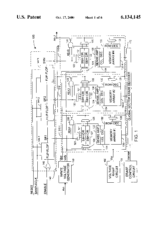
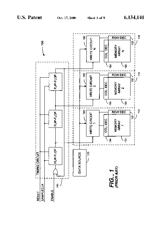
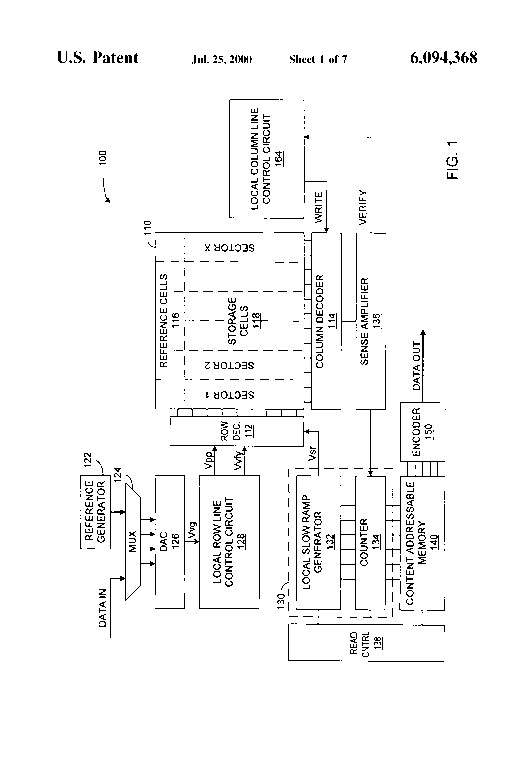
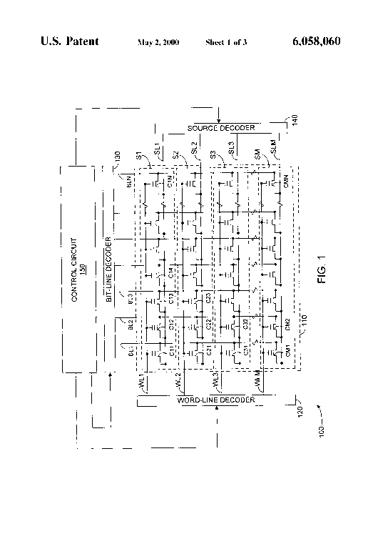
Drawing 1 of 4

US 5,943,283

Drawing 1 of 4

Expanded drawing 1 of 4 from US 5,943,283, Address scrambling in a semiconductor memory
High-resolution patent drawing

US 5,943,283

Address scrambling in a semiconductor memory

Filed
December 5, 1997
Granted
August 24, 1999
Assignee
Sandisk
Previous Assignee
Invox
Inventors
Sau C. Wong, Hock C. So

Abstract

A semiconductor memory includes a memory array and an address scrambler. The address scrambler maps sequential input addresses to non-sequential physical addresses for the memory array. In one embodiment, the address scramble includes circuitry that implements a one-to-one function mapping of the logical addresses to physical addresses. Alternatively, the address scrambler includes a pseudo-random series generator that generates a pseudo-random series for the physical addresses. In either case, consecutive memory accesses that would logically correspond to a single row or column are scattered among multiple rows and columns to diminish the length of a gap in a data sequence that would otherwise occur as a result of a defective row or column. For flash memory, the mapping can be restricted so that logical addresses for a sector map to physical address for the same or another sector. The scrambler optionally includes a volatile storage for a key or access code that selects the mapping or series used for determining the physical addresses. The access code used when recording must also be used during playback or the correct data will not be accessed.

View on Google Patents ↗
View Full PatentComplete archived record · 4 figures · 48 description paragraphs · 20 claims

Patent record

Source
Google Patents
Publication
US5943283A
Application
US08/986,210
Priority
December 5, 1997
Prior art date
December 5, 1997
Publication date
August 24, 1999
Legal status
Expired - Lifetime
Original assignee
Invox Technology Inc
Current assignee
SanDisk Technologies LLC
Prior art keywords
memory, address, sequence, addresses, scrambler
Source retrieved
July 20, 2026

Classifications

  • GPHYSICS
  • G06COMPUTING OR CALCULATING; COUNTING
  • G06FELECTRIC DIGITAL DATA PROCESSING
  • G06F12/00Accessing, addressing or allocating within memory systems or architectures
  • G06F12/14Protection against unauthorised use of memory or access to memory
  • G06F12/1408Protection against unauthorised use of memory or access to memory by using cryptography
  • G06F21/00Security arrangements for protecting computers, components thereof, programs or data against unauthorised activity
  • G06F21/70Protecting specific internal or peripheral components, in which the protection of a component leads to protection of the entire computer
  • G06F21/78Protecting specific internal or peripheral components, in which the protection of a component leads to protection of the entire computer to assure secure storage of data
  • G06F21/79Protecting specific internal or peripheral components, in which the protection of a component leads to protection of the entire computer to assure secure storage of data in semiconductor storage media, e.g. directly-addressable memories
  • G11INFORMATION STORAGE
  • G11CSTATIC STORES
  • G11C8/00Arrangements for selecting an address in a digital store
  • G11C8/20Address safety or protection circuits, i.e. arrangements for preventing unauthorized or accidental access

Figures

4 plates

Figure 1 of 4 from US 5,943,283, Address scrambling in a semiconductor memory
Figure 01Full resolution ↗
Figure 2 of 4 from US 5,943,283, Address scrambling in a semiconductor memory
Figure 02Full resolution ↗
Figure 3 of 4 from US 5,943,283, Address scrambling in a semiconductor memory
Figure 03Full resolution ↗
Figure 4 of 4 from US 5,943,283, Address scrambling in a semiconductor memory
Figure 04Full resolution ↗

Description

BACKGROUND

1. Field of the Invention

This invention relates to semiconductor memory and to methods and circuits for storing data in semiconductor memory at addresses selected to reduce the noticeable effects of defects and to memory with built-in security against unauthorized access of stored data.

2. Description of Related Art

Some semiconductor memory systems can record and playback continuous analog signals such as audio or image signals. In such systems, a recording process takes samples (i.e., instantaneous measurements of the level) of an analog signal to generate a data sequence that the semiconductor memory stores.

Depending on the type of memory, each sample is stored in digital form with one or more bits per memory cell or in analog form with one sample per memory cell. Such memory systems often include an address counter which indicates an address for storage of a sample in a data sequence. The address counter increments the address each time a sample is written so that samples are written at consecutive addresses. To play or recreate the recorded analog signal, the data sequence is read from the semiconductor memory in the sequential order of the recording, and samples read are sequentially converted to levels in an output signal.

Generally, a semiconductor memory includes an array of memory cells arranged in rows and columns and partitioned into independently addressable storage locations. Conventionally, each storage location corresponds to one or more memory cells in a row of the array. An address for a storage location identifies the row and the column associated with a memory cell in the storage location. Commonly, the most significant bits of an address form a row address that identifies the row containing the storage location, and the least significant bits of the address form a column address that identifies a column corresponding to one of the memory cells in the storage location. Often, when storing a sequence of samples to consecutive memory addresses, the column address is sequentially incremented, and the row address remains constant until the column address reaches the last position in the row. This fills a row of memory cells before starting writes to the next row.

For an audio recording and playback application, when a row or large number of adjacent cells in a row are defective, the defective cells contain unpredictable or incorrect values; and during signal playback, noticeable deadtime, static, or signal distortion appears in the portion of the signal recorded in defective memory cells. If all or a large number of memory cells in a column are defective, an error occurs in the signal played back each time a sample is read from a storage location including a defective memory cell. A column error thus results in periodic errors in the played-back signal where the period of the errors depends on the time required to read samples from a row. The errors may cause a repeating "pop" or "click" in a played-back sound. Periodic errors are undesirable because the human ear is attuned to detect such noise.

To handle hard defects (i.e., defects that are detectable by testing), most memories include redundant rows and columns of memory cells with redundant decoding circuits. When a defective row, a defective column, a number of defective adjacent memory cells, or even a single defective memory cell is detected during testing of a memory IC, a redundant row or column can be activated to replace the defective cells. Replacing defects in this manner increases memory cost because the redundant circuits increase integrated circuit area and because activation of the redundant circuits typically requires additional processing steps, such as laser programming during or after testing. Furthermore, a memory may still have latent defects or soft errors, which appear only after a specific period of operation of the memory. In the normal test flow, these defects typically cannot be detected as requiring replacement. Methods and circuits are thus sought to handle defects in semiconductor memory and record-and-playback systems and avoid lengthy disruptions or periodic errors that result from memory array defects.

SUMMARY

In accordance with the invention, sequential data such as samples representing an audio signal are stored in non-sequential storage locations. As a result, row and column defects cause distributed errors. The distributed errors are less noticeable and more easily corrected using filters or, for digital memory, error correction codes. The address selection for data storage can be such that neither row nor column defects cause lengthy dead time or periodic errors in a played-back signal. Instead, row defects and column defects cause pseudo-random noise which in audio signals is less noticeable. To implement record and playback processes in accordance with an embodiment of the invention, an address scrambler maps input or logical addresses to physical addresses for a memory array. The mapping is such that consecutive logical addresses are not mapped to the same physical row or column in an array.

In accordance with another aspect of the invention, the address scrambler selects a mapping from logical addresses to physical addresses based on a user-provided key or access code. Accordingly, a signal such as a recorded sound or voice signal is unintelligible when played back unless the user provides the same key for playback as was used for the recording. Accordingly, the system provides hardware-based security against unauthorized playback of recorded messages.

One memory system in accordance with an embodiment of the invention includes a memory array, an address counter that generates sequential logical addresses for record and playback operations, and a scrambler coupled to address counter and the memory array. The scrambler maps sequential logical addresses from the counter to non-sequential physical addresses for the memory array. The scrambler includes arithmetic logic that implements a one-to-one mapping of the logical addresses to physical addresses in the array. For flash memory embodiments, the mapping can be restricted so that logical addresses for a sector map to physical address for the same or another sector. In a specific embodiment, the scrambler includes an adder that combines a logical column address and a logical row address in generating a physical row or column address. The scrambler alternatively or additionally includes a mixer that permutes or mixes the bits of the logical row and column addresses. The scrambler may optionally include a register for a key or access code that selects the bit permutation and more generally selects the function implemented for mapping logical addresses to physical addresses.

Another memory system includes an address generator that generates a pseudo-random sequence. The address generator directs a sequence of memory accesses to storage locations that are scattered throughout a memory array or a sector within a memory array.

BRIEF DESCRIPTION OF THE DRAWINGS

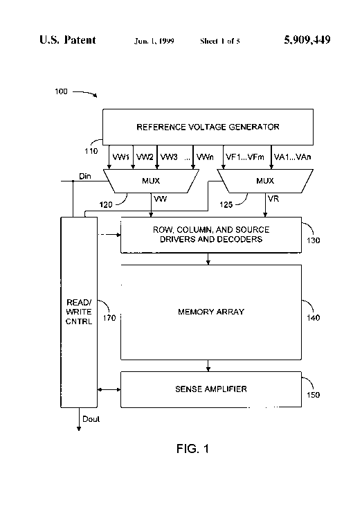
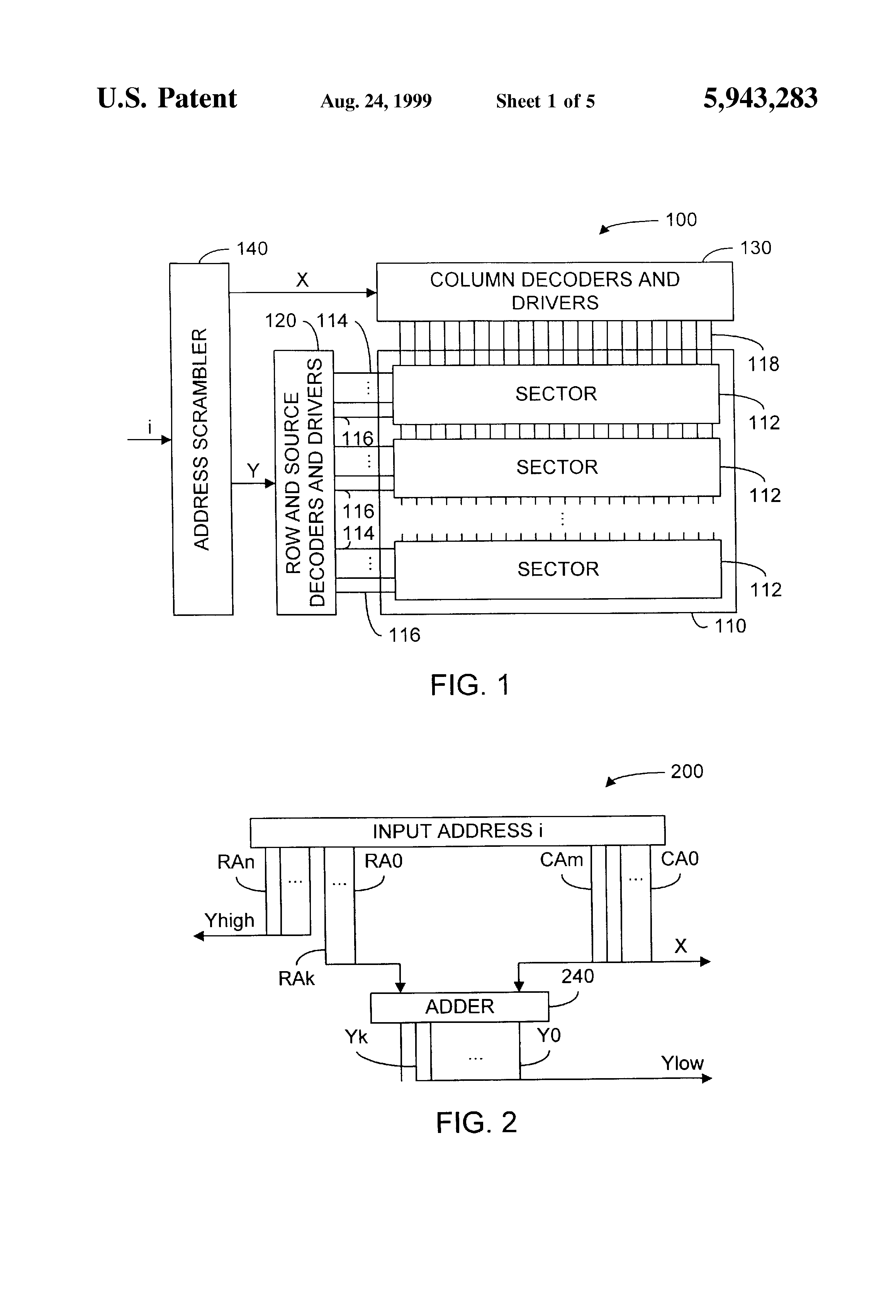
FIG. 1 shows an analog flash memory system that includes row-based sectors and address scrambling in accordance with an embodiment of the invention.

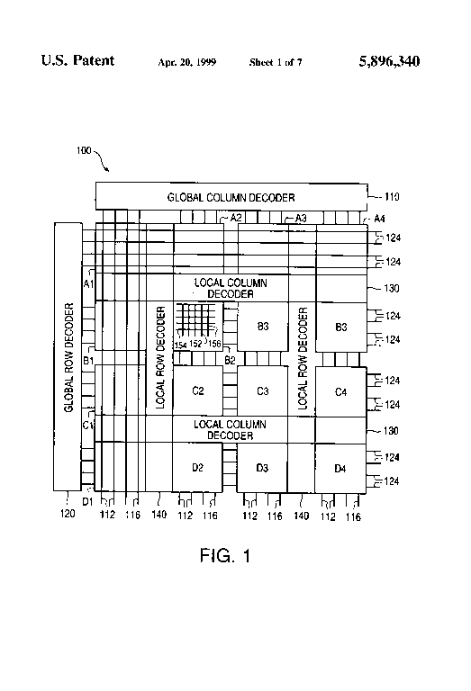
FIG. 2 shows an address scrambler for the memory of FIG. 1.

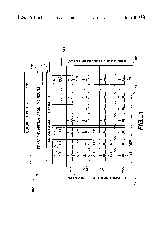
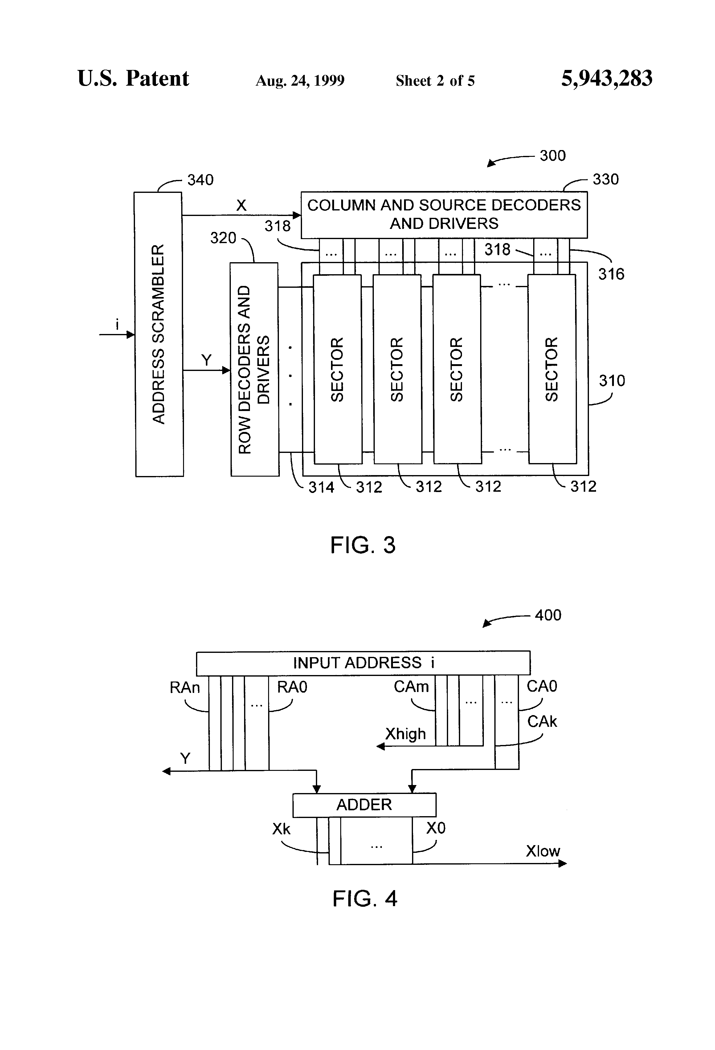
FIG. 3 shows an analog flash memory system that includes column-based sectors and address scrambling in accordance with an embodiment of the invention.

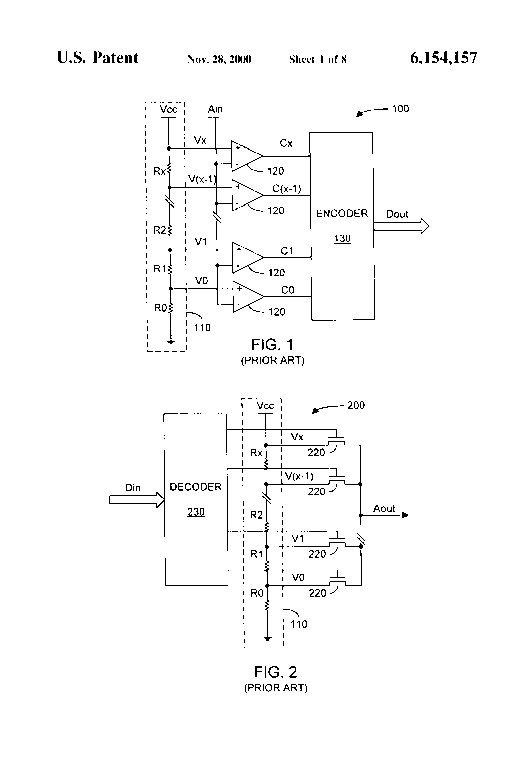
FIG. 4 shows an address scrambler for the memory of FIG. 3.

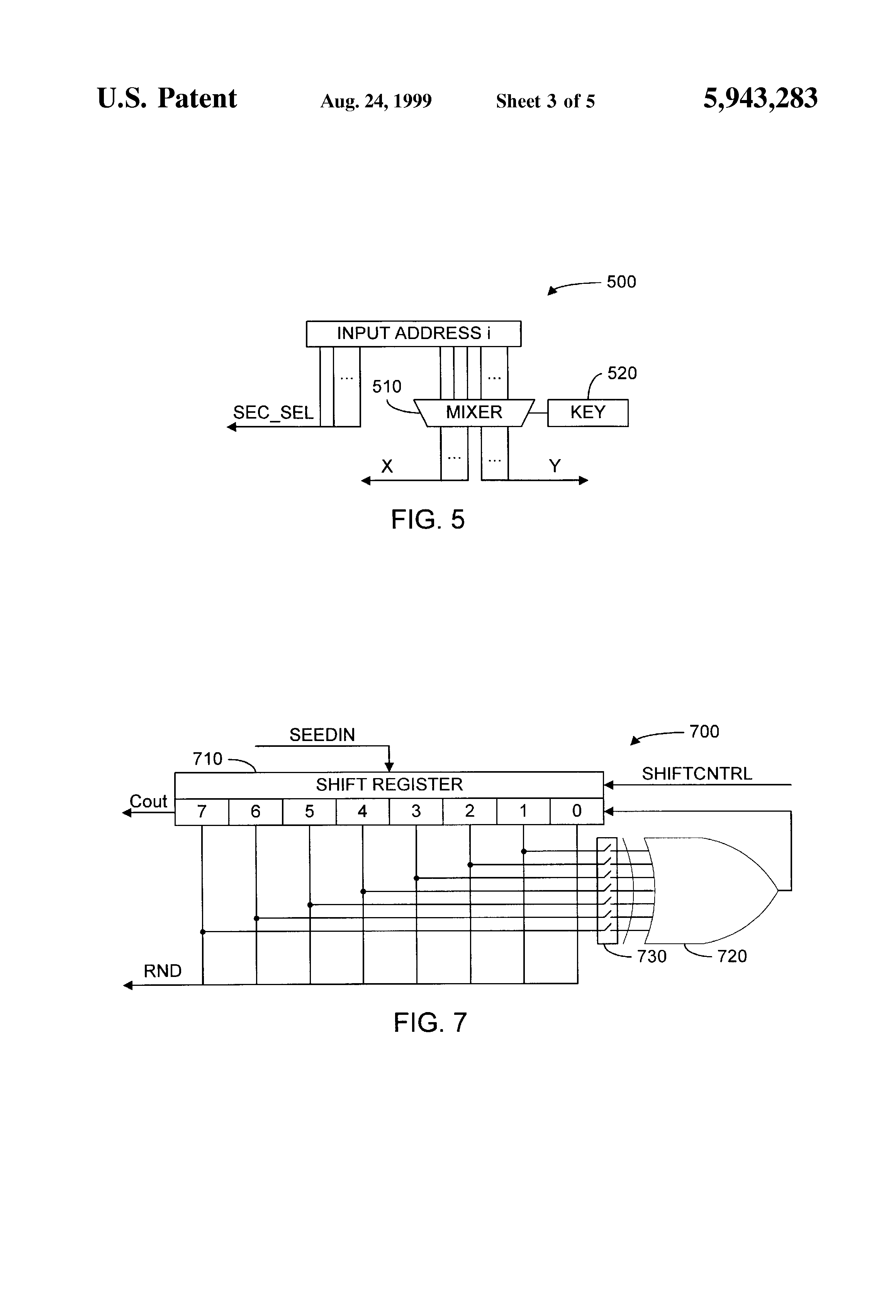
FIG. 5 shows an address scrambler that permutes bits of an input logical address.

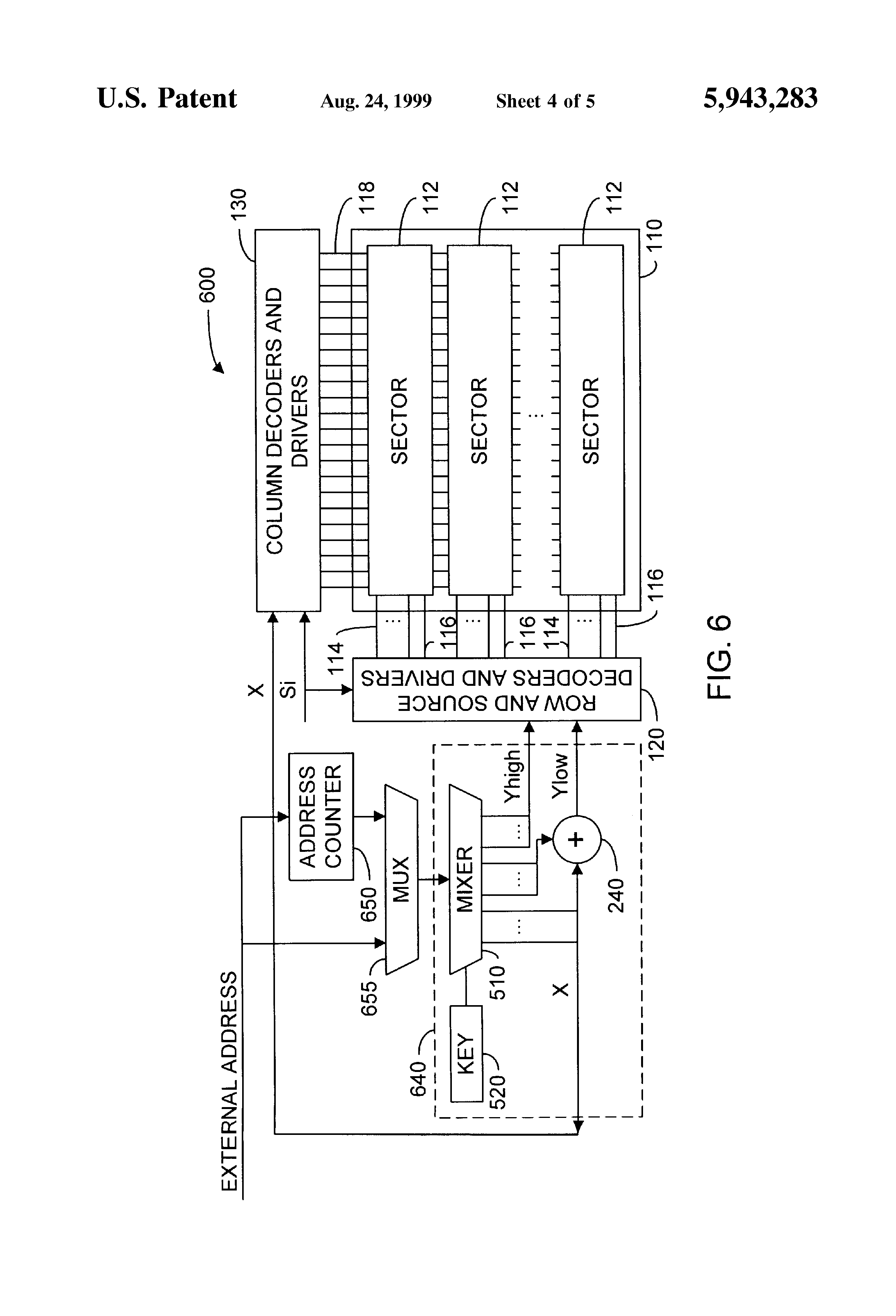
FIG. 6 shows a memory system in accordance with an embodiment of the invention including an address counter for recording and playing analog signals.

FIG. 7 shows a generator of a non-repeating random series multi-bit digital signal.

FIG. 8 shows a memory system in accordance with an embodiment of the invention including a generator such as in FIG. 7 to scramble addresses.

Use of the same reference symbols in different figures indicates similar or identical items.

DETAILED DESCRIPTION OF THE PREFERRED EMBODIMENTS

In accordance with an aspect of the invention, a memory system includes an address scrambler that converts sequential logical addresses to non-sequential physical addresses for a memory array. Thus, record and playback operations use sequential input addresses for a data sequence but access storage locations that are not sequential in a row or column. Accordingly, use of memory with defects such as column and row defects do not cause loss of lengthy runs of consecutive data values. Instead, row defects and column defects cause scattered errors. Such scattered errors are tolerable in error tolerant memory applications such as voice, sound, and digital imaging. Accordingly, the cost of a record-and-playback system can be reduced by eliminating redundant rows, columns, and decode circuits and eliminating the processing and testing steps that activate redundant circuits.

FIG. 1 shows a semiconductor memory 100 in accordance with an embodiment of the invention. Memory 100 is an analog flash memory which includes an array 110 of memory cells, where each memory cell in the array is an independently addressable storage location capable of storing an analog value. Flash memory such as flash EPROM or flash E2 PROM is non-volatile and has independently erasable sectors 112 of memory cells. Alternative embodiments of the invention employ different memory architectures as in non-volatile memories such as EPROM and E2 PROM and volatile memories such as DRAM and SRAM, and each memory cell can store an analog value or one or more bits of a digital value.

Array 110 contains rows and columns of memory cells such as floating gate or split gate transistors having control gates coupled to row lines 114 and drains coupled to column lines 118. Each row line 114 connects to an associated row of memory cells in array 110. Each column line 118 connects to an associated column of memory cells in array 110. Array 110 is also divided into independently erasable sectors 112, where each sector contains one or more rows of memory cells. FIG. 3 shows an alternative flash memory architecture employing sectors that contain columns rather than rows of memory cells. Each sector 112 in array 110 has a source line 116 that connects to the sources of the memory cells in the sector. Row and source decoders and drivers 120 connect to row lines 114 and source lines 116 and apply voltages to selected row and source lines as required for erase, write, and read operations. Column decoders and drivers 130 connect to column lines 118 and apply voltages to selected column lines as required for erase, write, and read operations. U.S. patent application Ser. No. 08/781,741, entitled "Source Biasing in Non-Volatile Memory having Row-Base Sectors", describe decoders and drivers 120 and 130 for specific embodiments of the invention and is incorporated by reference herein in its entirety.

During a read or write to memory array 110, row decoder 120 and column decoder 130 respectively require a row address and a column address that respectively identify a row line and a column line coupled to the memory cell (i.e., storage location) being read or written. In accordance with an aspect of the invention, memory 100 includes an address scrambler 140 that generates a physical address from an input logical address i. The physical address contains a physical row address Y and a physical column address X that respectively represent row and column numbers for a memory cell in array 110. Input address i may be an address signal input to memory 100 for random access to memory cells in array 110 or may be from an on-chip counter that generates a sequential address signal for recording or playing back a data sequence. Input address i logically identifies a storage location being accessed but is not required to contain the physical row and column number identifying a location in array 110. Instead, scrambler 140 converts the input address i to the physical address for the storage location being accessed.

Scrambler 140 can employ a variety of scrambling or encryption techniques when converting an input (or logical) address to a physical address. Generally, when input address i is restricted to the address space of array 110, scrambler 140 implements a one-to-one mapping of the address space of array 110 back onto itself. With a one-to-one mapping, a user uses input address i for memory accesses, and the actions of scrambler 140 are transparent to the user. Scrambler circuits implementing such mappings can take a variety of forms particularly because of the large number of possible mappings for a typical size memory array.

For flash memory embodiments of the invention such as memory 100, scrambler 140 preferably maps all input addresses logically associated with a sector to physical addresses within a single sector, either the same sector or another sector. This keeps data targeted for a sector together so that erasing a sector erases the data targeted to be together. For example, in an audio recording and playback system, an audio signal is represented as a continuous sequence of samples. It is often desirable to erase only a specific duration of the audio signal by erasing a portion of the sequence. If consecutive samples of an audio signal are stored in the same sector, erasing a sector erases only a piece of the audio signal but leaves the remainder of the audio signal intact. The duration of the portion erased depends on the size of each sector in the memory. Accordingly, a mapping that maps a sector onto a sector preserves the ability to erase selected portions or periods of a recorded signal.

FIG. 2 shows an embodiment of an address scrambler 200. Scrambler 200 splits input logical address signal i into (m+1) least significant bits CA0 to CAm and (n+1) most significant bits RA0 to RAn. Bits CA0 to CAm represent an input logical column address CA, and bits RA0 to RAn represent an input logical row address RA. For scrambler 200, the physical column address X for memory array 110 is the same as input column address CA, but the physical row address Y is a combination of input column address CA and input row address RA such that row address Y changes when input row address RA is constant and input column address CA changes. Thus, scrambler 200 maps sequential input addresses having a single value for input row address RA to several different rows in array 110.

Scrambler 200 uses an adder 240 to generate physical row address Y for array 110 from input row and column addresses RA and CA. The most significant bits of row address Y identify a sector in array 110 and are the same as bits RA(k+1) to RAn of input row address RA. Accordingly, scrambler 200 does not change the sector that input address i identifies for access but maps sequential input logical addresses corresponding to memory cells located along diagonals in the sector. Alternatively, scrambler 200 could map the sector identified by input bits RA(k+1) to RAn to a different sector using one-to-one mapping of sectors onto themselves. Adder 240 adds input column address CA to the (k+1) least significant bits RA0 to RAk of input row address RA to generate (k+1) least significant bits Y0 to Yk of row address Y, where each sector 112 contains (k+1) rows of memory cells. Any carry bits are ignored. The least significant bits Ylow of row address Y identify a row within a sector. Since adder 240 adds input row address RA and input column address CA together when generating physical row address Y, both column address X and row address Y change when input address i increments, and two consecutive values of input address do not map to the same physical row.

A potential concern for scrambler 200 arises when a sequence of input addresses increments input row address RA and keeps input column address CA constant. A sequence of input addresses with constant input column address CA is a logical column. Scrambler 200 maps such a sequence of input addresses to the same physical column so that the data sequence is written or read from a single physical column. In such cases, a column defect can cause errors in a long run of sequential data. However, with the input column address CA being defined as the least significant bits of the input address i, the natural ordering of input address corresponds to a row and not a column. An address counter, for example, which could supply the input address i when writing or reading a data sequence most conventionally sequentially adds to the least significant bits of input address i which form column address CA. Sequential input addresses from such a counter correspond to storage locations scattered across the physical rows in a sector.

FIG. 3 shows a semiconductor memory 300 including a memory array 310 having sectors 312, where each sector 312 contains one or more columns of analog memory cells. Each sector 312 in array 310 has a source line 316 that connects to the sources of the memory cells in the sector. Source and column decoders and drivers 330 connect to source lines 316 for sectors 312 and to column lines 318 for columns of memory cells in array 310. Row decoder and drivers 320 connect to row lines 314 for rows of memory cells in array 310. Using circuits and processes known in the art, decoders and drivers 320 and 330 apply voltages to selected row, column, and source lines as required for erase, read, and write operations. Since each sector of array contains several columns, writing sequential data to column-by-column may be more convenient than writing the data row-by-row. An address scrambler 340 provides row and column address signals Y and X to identify a memory cell selected for a read or write operation. Address scrambler 340 preferably maps logical columns as identified by a constant input logical column address CA to randomly distributed columns in a sector 312.

FIG. 4 shows an embodiment of an address scrambler 400 for memory 300. Scrambler 400 is the same as scrambler 200 of FIG. 2, except that the roles of input row address RA and input column address CA are reversed from those described above in regard to FIG. 2. In FIG. 4, k is the number of columns in a sector 312. Scrambler 400 prevents a data sequence with constant input column address CA from being mapped to a single physical column. Instead such a data sequence is scattered across the columns of a sector.

An advantage of scattering write addresses across row or columns of a flash memory array is reduction in the accumulated disturbance of data in the first rows of the array. In particular, writing short data sequences conventionally only writes to the first rows, and programming voltages applied to row lines disturb data values stored in memory cells in the first rows. Address scrambling spreads the disturbance across the array even for short data sequences. Scramblers 200 and 400 respectively scramble the row and column addresses. Scrambling only the row address or only the column address may have a speed advantage in a memory where column or row decoding is relatively slow. For example, time delay cause by scrambling row addresses may be partially or totally hidden in read or write times that are delayed by slower column decoding circuits. As discussed above, scrambling only rows or only columns is useful for eliminating long runs of lost data caused respectively by row defects or column defects. A disadvantage of using scrambler 200 with an array having a row defect or using scrambler 400 with an array having a column defect is the creation of a periodic error. The periodic error may be noticeable in an analog signal such as an audio signal. The periodic nature of the error can be eliminated using a scrambler that is more random than scrambler 200 or 400.

FIG. 5 illustrates an alternative address scrambler 500 in accordance with an embodiment of the invention. Address scrambler 500 includes a mixer 510 having input terminals coupled to some or all of the bits of input address i. The bits of input address i that are not coupled to mixer 510 form a signal SEC13 SEL that identifies a sector in a flash memory. Signal SEC13 SEL may be, for example, the most significant bits of the logical row or column address depending on the sector configuration. Mixer 510 performs a one-to-one mapping of values of input address i to the values of an output address signal having parts X and Y. For example, mixer 50 can permute or reorder bits from input address i so that long runs of consecutive input address are not in the same row or column. Preferably, mixer 510 swaps some (but not all) of the bits of logical row address RA and with some (but not all) of the bits of logical column address CA so that neither a logical column nor a logical row is mapped to a physical column or row.

Table 1 shows example permutations of four bits of an input address.

Example permutation 1, which swaps all of the address bits of input row address RA with all of the bits of input column address CA, maps a logical row to a physical column. Accordingly, if a data sequence is written to a logical row and example permutation 1 is used, the data sequence is stored in a physical column. This is undesirable because a column defect would cause loss of a lengthy sequence of consecutive data. Example permutation 2 and 3, which swap some of the bits of input row address RA with some of the bits of input column address CA, provide better mixing of a logical row into multiple physical columns and rows.

As a further aspect of the invention, scrambler 500 includes a storage element or register 520 for a key or access code. Register 520 can be user-accessible volatile memory to permit a user to change the key for writing or reading data in a memory. Based on the value of key in register 520, mixer 510 selects from among the set of suitable permutations input bits. A typical memory containing, for example, 512 physical row addresses and 512 column address has 18-bit addresses and about 6.4×10¹⁵ possible permutations of address bits. If the memory has a flash architecture with 16 rows or columns per sector, 13-bits are available for permutations which keep data values within a sector, and there are about 6.2×10⁹ possible permutations. Suitable permutations can be selected based on the effectiveness of the permutation at mixing sequential logical addresses in physical rows and columns and/or the similarity or dissimilarity to other suitable permutations. While not all of the possible permutation are suitable, a large number of suitable permutations should be available for a typical memory. This permits a large number of possible access codes to select a specific one of the suitable permutations.

As an alternative to permuting bits of the input signal, mixer 510 can be any logic that implements a one-to-one, "random" mapping of input signal values to output signal values. The output signal values can correspond to only a portion of the available memory storage and are not required to contain the same number of bits as are in the input signals. Techniques known for data encryption, which often uses keys, can also be employed for scrambling individual addresses or series of addresses. Circuits implementing one-to-one mappings are well known in the art. Mixers that implement simple permutations of bit values are only one example. Alternatively, a mapping circuit can include inverters on selected bits, parity check circuits that enable one permutation and set of inversions for even parity values and another permutation and set of inversions for odd parity values, or any random logic that provides a one-to-one mapping. Whether, a one-to-one mapping is sufficiently random depends on how well the mapping scatter sequential input values across and array or sector. In such embodiments, memory location 520 can either select a mapping circuit from among a group of circuits implementing "random" mappings and/or provide parameters for the mapping circuit.

FIG. 6 shows a memory 600 permitting random access and writing and reading of data sequences, for example, for recording and playing of audio signals. Memory 600 includes row and source decoders and drivers 120, column decoders and drivers 130, and an array 110 having row-based sectors 112 as described above in regard to FIG. 1. For audio recording, an analog signal from a microphone or other device is sampled to generate sequential samples Si, and decoders and drivers 120 and 130 select and apply voltages to a memory cell in array 110 to set the threshold voltage of the memory cell at a level indicating one of samples Si. Memory 600 is placed in sequential mode where a multiplexer 655 provides an address signal from an address counter 650 to address scrambler 640. In this mode an external address initializes address counter 650 to a starting point of a sequential access, and counter 650 increments the logic address when each sample Si is written to memory array 110. Address scrambler 640 generates the physical addresses for selection of storage for samples Si. In particular, scrambler 640 converts the logical address from counter 650 to a physical address including physical column address X and physical row address Y. Sequential samples Si are written to memory array 110 at storage locations that the physical addresses identify.

Scrambler 640 includes mixer 510 that mixes all of the bits of the logical addresses using a one-to-one mapping selected according to a user-programmable key value from register 520. The key value is user-provided and selects one of a set suitable mappings. Output from mixer 510 includes a group of bits selected as the physical column address X, a group of bits Yhigh selected for the most significant bits of row address Y, and a group of bits that adder 240 adds to the physical column address X to generate the least significant bits Ylow of physical row address Y. Bits Yhigh select the sector to which the current sample is written. Accordingly, to keep consecutive samples having the same logical sector in the same physical sector, bits in Yhigh must only depend on the most significant bits of logical address (i.e., of the logical row address Y). The number of rows in a sector 112 determines the maximum number of bits in Ylow. Typically, although not necessarily, the maximum value of bits Ylow is equal to the number of rows in a sector. In an alternative embodiment, the key in register 520 selects the partition of row address Y between bits Ylow and bits Yhigh.

As noted above, suitable permutations or mappings of the logical address are selected according to the efficiency of scattering sequential address across the physical rows and columns. However, scrambler 640 includes adder 240 which further mixes sequential addresses. Accordingly, the net effect of adder 240 and mixer 510 must be considered. When security is a greater concern than reducing the effects of row or column defects, a set of suitable permutations or mappings includes permutations or mappings that provide incomprehensible playback when the key for playback differs from the key for recording.

For a playback operation, address counter 650 generates sequential logical addresses that scrambler 640 converts to physical addresses for reading memory array 110. Filters, a converter, and an amplifier (not shown) convert the samples read to an output analog audio signal which a speaker (not shown) coverts to sound. In order for the output audio signal to mimic the recorded signal, scrambler 640 must implement the same mapping during the playback operation as was used during the recording operation, that is, the user must provide the correct key.

For random access of memory array 110, memory 600 operates in a mode where multiplexer 655 provides the external address to scrambler 640. Scrambler 640 converts the external address to a physical address in array 110. Random access can be for any type of data and is not limited to sequential data or data representing an analog or continuous signal. The location of each datum in array depends on the key used when the datum was written and cannot be easily identified for reading without the appropriate key in register 520.

For scrambled random access to a memory, scrambler 640 maps logical addresses to physical address. However, when only sequential access is required, a scrambler can generate a random series without the need of an input address except to select a starting point of a sequential access. FIG. 7 illustrates a pseudo-random series generator 700 which includes a shift register 710, an XOR gate 720, and a programmable switch 730 and generates a pseudo-random series. Generator 700 has an 8-bit output signal RND that represents the content of shift register 710 and changes according to the pseudo-random series. Output signal RND and the content of shift register 710 are initialized accordingly to a non-zero input signal SEEDIN and change each time a control signal SHIFTCNTRL causes shift register 710 to perform a left shift. During a shift, a most significant bit shifts out of shift register 710 as an ignored carry bit Cout, and a bit from XOR gate 720 shifts into the least significant bit. XOR gate 720 generates an output bit that is 1 only when an odd number of the input bits are 1. Programmable switch 730 selects which bits from shift register 710 are input to XOR gate 720. Not all possible combinations of input bits generate a random series of suitable length. However, with bits 7, 3, 2, and 1 of shift register 710 connected to the input terminals of XOR gate 720, the content of shift register 710 takes on every value in a range from 1 to 255 before repeating any of the values. For a full 8-bit range of values (i.e., 0 to 255), a zero-valued signal (representing eight 0 bits) can be inserted at any point in the series in place of the output from shift register 710. While the zero-valued signal is asserted, the contents of shift register 710 is preserved so that the series can resume as normal when required.

Generator 700 is only one example of circuit that generates a pseudo-random series and can be varied in a variety of ways. For example, a right shift could be used. A larger or smaller shift register and an XOR gate coupled to the shift register can provide a different range for the pseudo-random series. W. H. Press, S. A. Teukolsky, W. T. Vetterling, and B. P. Flannery, "Numerical Recipes in C," 2nd edition, Cambridge University Press, 1992 describes pseudo-random number generators of this type using shifted values up to 100 bits in size.

Pseudo-random series generators like generator 700 are applicable in variety of ways to the circuits described herein. For example, for sequential memory access, the combination of adder 240, mixer 510, and address counter 650 as shown in FIG. 6 can be replaced with a pseudo-random series generator like generator 700 where the range of the random series is equal to the sector size. Storage location 520 provides seed signal SEEDIN to generator 700 at the start of the series for writing to or reading from a sector. Seed value SEEDIN may depend of the sector being accessed. The random series of addresses from the generator effectively eliminates long lapses and periodic errors caused by a row or column defect. In audio, for example, a row or column defect shows up as random noise rather than a periodic artifact or an interval of static. However, a seed value only selects a starting point for the random series, and an incorrect seed value may leave portions of a recording audible. Thus, security protection is minimal.

FIG. 8 shows a memory 800 having an alternative use of a random series generator 855 which is of the type shown in FIG. 7 but has a range matching the size of a sector 112 in memory array 110. Memory 800 is similar to memory 600 of FIG. 6 but has an address scrambler 840 that differs from address scrambler 640 of memory 600. In address scrambler 840, a sector counter 850 and series generator 855 provide the input address signal to mixer 510. For each memory location accessed, series generator 855 changes the output signal. Mixer 510 maps the bits of the signal from series generator 855 to a physical column address X and the low bits Ylow of row address Y. Sector counter 850 generates a sector count identifying the sector being accessed and increments or changes the sector count at the start of an access of a sector. To keep sequential samples Si together in a sector, mixer 510 has an output signal Yhigh that selects a sector 112 and is independent of the value from series generator 855. However, mapping of the series from generator 855 to signals X and Ylow can depend on the sector as identified by sector counter 850. Mixer 510 and key 520 provide additional user selectable scrambling for improved security over use of generator 855 without a mixer. A disadvantage of memory 800 is the difficulty of providing random access for data that was sequentially stored or is to be sequentially read. For example, finding a particular address may require several shifts in generator 855.

Although the invention has been described with reference to particular embodiments, the description is only an example of the invention's application and should not be taken as a limitation. In particular, even though much of preceding discussion was aimed at mappings implemented using permutations and additions, alternative embodiments of the invention can include any circuit that is capable of performing a mapping from a logical address space to a physical address space. Further, although use of a key value was discussed primarily in the context of selecting a permutation of bits of a logical address, such keys can be used generally as a parameter to select from among a family of mappings. Further, although embodiments of the invention were described in the context of data associated with sequential audio samples, embodiments of the invention are applicable to any organized or ordered data structure not limited to time ordered samples. For example, financial, medical, or other personal data can be stored in an access card containing a memory with address scrambling in accordance with the invention. In the event that the access card is lost or stolen, unauthorized retrieval of the stored information in meaningful form is difficult since logical addresses of data and therefore the meaning of the data stored depends on the access code. Further, data can be encrypted before storage using data encryption and stored using address scrambling or encryption as described herein. Various other adaptations and combinations of features of the embodiments disclosed are within the scope of the invention as defined by the following claims.
Claims (20)

  1. A memory comprising: an array of memory cells; address decoders coupled to the array; and a scrambler coupled to the address decoders, wherein the scrambler converts a first address signal that is input to the scrambler to a second address signal that is provided to the address decoders to select a storage location in the array, the scrambler by converting the first address signal reduces effects of row and column defects in the memory.
  2. The memory of claim 1, wherein: the scrambler converts a first sequence of values of the first address signal to a second sequence of values of the second address signal: the first sequence, if applied directly to the address decoders, would correspond to storage locations in a row in the array; and the second sequence, when applied to the address decoders, corresponds to storage locations in a plurality of rows of the array.
  3. The memory of claim 1, wherein: the scrambler converts a first sequence of values of the first address signal to a second sequence of values of the second address signal; the first sequence, if applied directly to the address decoders, would correspond to a single column of storage locations in the array; and the second sequence, when applied to the address decoders, corresponds to storage locations in a plurality of columns of the array.
  4. The memory of claim 1, further comprising a counter coupled to the scrambler, wherein the first address signal represents a count stored in the counter.
  5. The memory of claim 4, further comprising a control circuit coupled to the counter and capable of controlling the memory for execution of a record operation, wherein during the record operation, a sequence of data values are written to the array and the counter increments the first address signal for each data value written.
  6. The memory of claim 4, further comprising a control circuit coupled to the counter and capable of controlling the memory for execution of a playback operation, wherein during the playback operation, a sequence of data values are read from the array and the counter increments the first address signal for each data value read.
  7. The memory of claim 1, wherein the scrambler is operable in a plurality of modes, each mode being associated with a different mapping of possible values of the first address signal to the possible values of the second address signal, and wherein the memory further comprises a mode selection circuit that selects the operating mode of the scrambler.
  8. The memory of claim 7, wherein the mode selection circuit comprises storage for an access code that identifies the operating mode of the scrambler.
  9. The memory of claim 1, wherein the first address signal and the second address signal are digital signals of equal width.
  10. The memory of claim 1, wherein the array of memory cells, the address decoders, and the scrambler are components of a single monolithic integrated circuit.
  11. The memory of claim 1, wherein: the array includes a plurality of independently erasable sectors; the scrambler converts a first sequence of values of the first address signal to a second sequence of values of the second address signal; the first sequence, if applied directly to the address decoders, would identify storage locations in a single sector; and the second sequence, when applied to the address decoders, identifies storage locations in a single sector.
  12. The memory of claim 11, wherein the first sequence of values identifies the same sector that the second sequence of values identifies.
  13. The memory of claim 11, wherein the first sequence of values and the second sequence of values identify different sectors.
  14. A method for operating a memory, comprising: generating a first address signal that represents a first sequence of addresses, wherein each address in the first sequence comprises a row address and a column address, and the row addresses or the column addresses are constant throughout the first sequence; converting the first address signal to a second address signal that represents a second sequence of addresses with neither row addresses nor column addresses being constant for the second sequence; and accessing a sequence of storage locations in the memory that corresponds to the second sequence of addresses and to a sound signal, wherein accessing data according to the second sequence of addresses instead of the first sequence of addresses reduces audible effects that row and column defects in the memory have on sound reproduced from the data in the sequence of storage locations.
  15. The method of claim 14, wherein accessing the storage locations comprises writing values from a data sequence to the storage location identified by the second sequence of addresses.
  16. The method of claim 14, wherein accessing the storage locations comprises reading values of a data sequence from the storage location identified by the second sequence of addresses.
  17. The method of claim 14, further comprising: identifying an access code for the operation of the memory; and selecting from a plurality of mappings a mapping that corresponds to the access code, wherein converting the first address signal comprises applying the selected mapping to the addresses in the first sequence to generate the addresses in the second sequence.
  18. The method of claim 14, wherein the converting is performed by a circuit in an integrated circuit containing the memory.
  19. A record-and-playback system comprising: an array of memory cells; address decoders coupled to the array; and a pseudo-random series generator coupled to the address decoders, wherein: the pseudo-random series generator generates an address signal that is provided to the address decoders for a series of memory accesses identifying a data sequence corresponding to a sound; for the series of memory accesses, values of the address signal form a pseudo-random series; and accessing the memory according to the pseudo-random series reduces audible effects that row and column defects in the memory have on the sound when reproduced from data in the memory.
  20. The record-and-playback system of claim 19, further comprising volatile storage coupled to the pseudo-random series generator, wherein the volatile storage stores an access code, and the pseudo-random series generator selects the pseudo-random series according to the access code.

Publications

Related applications (3)

  1. US08/986,210

    Priority application

  2. US08/986,210

    Claims priority

  3. US08/986,210

    Patent family

Record timeline

  1. Application filed by Invox Technology Inc

  2. Priority to US08/986,210

  3. Assigned to INVOX TECHNOLOGY, INC.

  4. Application granted

  5. Publication of US5943283A

  6. Assigned to SANDISK CORPORATION

  7. Assigned to SANDISK TECHNOLOGIES INC.

  8. Assigned to SANDISK TECHNOLOGIES LLC

  9. Anticipated expiration

  10. Expired - LifetimeCurrent

Legal events

  1. AS

    Assignment

    Owner name: INVOX TECHNOLOGY, INC., CALIFORNIA

    Free format text: ASSIGNMENT OF ASSIGNORS INTEREST;ASSIGNORS:WONG, SAU C.;SO, HOCK C.;REEL/FRAME:008893/0787

    Effective date: 19971205

  2. STCF

    Information on status: patent grant

    Free format text: PATENTED CASE

  3. AS

    Assignment

    Owner name: SANDISK CORPORATION, CALIFORNIA

    Free format text: ASSIGNMENT OF ASSIGNORS INTEREST;ASSIGNOR:INVOX TECHNOLOGY;REEL/FRAME:011812/0888

    Effective date: 19990920

  4. FEPP

    Fee payment procedure

    Free format text: PAYOR NUMBER ASSIGNED (ORIGINAL EVENT CODE: ASPN); ENTITY STATUS OF PATENT OWNER: LARGE ENTITY

  5. FEPP

    Fee payment procedure

    Free format text: PAT HOLDER NO LONGER CLAIMS SMALL ENTITY STATUS, ENTITY STATUS SET TO UNDISCOUNTED (ORIGINAL EVENT CODE: STOL); ENTITY STATUS OF PATENT OWNER: LARGE ENTITY

  6. REFU

    Refund

    Free format text: REFUND - SURCHARGE, PETITION TO ACCEPT PYMT AFTER EXP, UNINTENTIONAL (ORIGINAL EVENT CODE: R2551); ENTITY STATUS OF PATENT OWNER: LARGE ENTITY

    Free format text: REFUND - SURCHARGE FOR LATE PAYMENT, SMALL ENTITY (ORIGINAL EVENT CODE: R2554); ENTITY STATUS OF PATENT OWNER: LARGE ENTITY

  7. REMI

    Maintenance fee reminder mailed

  8. FPAY

    Fee payment

    Year of fee payment: 4

  9. SULP

    Surcharge for late payment

  10. FPAY

    Fee payment

    Year of fee payment: 8

  11. FPAY

    Fee payment

    Year of fee payment: 12

  12. AS

    Assignment

    Owner name: SANDISK TECHNOLOGIES INC., TEXAS

    Free format text: ASSIGNMENT OF ASSIGNORS INTEREST;ASSIGNOR:SANDISK CORPORATION;REEL/FRAME:026224/0398

    Effective date: 20110404

  13. AS

    Assignment

    Owner name: SANDISK TECHNOLOGIES LLC, TEXAS

    Free format text: CHANGE OF NAME;ASSIGNOR:SANDISK TECHNOLOGIES INC;REEL/FRAME:038813/0004

    Effective date: 20160516

Patent citations (4)

  1. US5081675A

    System for protection of software in memory against unauthorized use

    Kitti Kittirutsunetorn · January 14, 1992 · Examiner cited

  2. US5587954A

    Random access memory arranged for operating synchronously with a microprocessor and a system including a data processor, a synchronous DRAM, a peripheral device, and a system clock

    Texas Instruments Incorporated · December 24, 1996 · Examiner cited

  3. US5587954B1

    Random access memory arranged for operating synchronously with a multiprocessor and a system including a data processor a synchronous dram a peripheral device and a system clock

    Texas Instruments Inc · June 23, 1998 · Examiner cited

  4. US5765197A

    Method and system for authentication of a memory unit for a computer system

    International Business Machines Corporation · June 9, 1998 · Examiner cited

Cited by (345)

  1. WO2000070620A1

    Memory array with address scrambling

    Giesecke & Devrient Gmbh · November 23, 2000 · Examiner cited

  2. US6671219B1

    Storage, storage method, and data processing system

    Hitachi, Ltd. · December 30, 2003 · Examiner cited

  3. US6415198B1

    Plasma etching of silicon using a chlorine chemistry augmented with sulfur dioxide

    Applied Materials, Inc. · July 2, 2002

  4. US6278633B1

    High bandwidth flash memory that selects programming parameters according to measurements of previous programming operations

    Multi Level Memory Technology · August 21, 2001

  5. US6330185B1

    High bandwidth multi-level flash memory using dummy memory accesses to improve precision when writing or reading a data stream

    Multi Level Memory Technology · December 11, 2001

  6. US6532556B1

    Data management for multi-bit-per-cell memories

    Multi Level Memory Technology · March 11, 2003 · Examiner cited

  7. US6363008B1

    Multi-bit-cell non-volatile memory with maximized data capacity

    Multi Level Memory Technology · March 26, 2002

  8. US6558967B1

    Multi-bit-per-cell memory system with numbers of bits per cell set by testing of memory units

    Multi Level Memory Technology · May 6, 2003

  9. US6856568B1

    Refresh operations that change address mappings in a non-volatile memory

    Multi Level Memory Technology · February 15, 2005

  10. US6522586B2

    Dynamic refresh that changes the physical storage locations of data in flash memory

    Multi Level Memory Technology · February 18, 2003

  11. US7079422B1

    Periodic refresh operations for non-volatile multiple-bit-per-cell memory

    Samsung Electronics Co., Ltd. · July 18, 2006

  12. US6396744B1

    Flash memory with dynamic refresh

    Multi Level Memory Technology · May 28, 2002

  13. US6754128B2

    Non-volatile memory operations that change a mapping between physical and logical addresses when restoring data

    Multi Level Memory Technology · June 22, 2004

  14. US6577534B2

    Non-volatile semiconductor memory device having a low defective rate

    Mitsubishi Denki Kabushiki Kaisha · June 10, 2003

  15. US7146528B2

    Simple fault tolerance for memory

    Honeywell International Inc. · December 5, 2006

  16. US20040153744A1

    Simple fault tolerance for memory

    Honeywell International, Inc. · August 5, 2004 · Examiner cited

  17. US6678836B2

    Simple fault tolerance for memory

    Honeywell International, Inc. · January 13, 2004

  18. US7254717B2

    Method and arrangement for protecting information

    Nokia Corporation · August 7, 2007

  19. WO2002071231A1

    Method and arrangement for protecting information

    Nokia Corporation · September 12, 2002 · Examiner cited

  20. US20040252575A1

    Method and arrangement for protecting information

    Tero Karkkainen · December 16, 2004 · Examiner cited

  21. US20040128458A1

    Method and device for protecting data transmission between a central processor and a memory

    Wolfgang Buhr · July 1, 2004 · Examiner cited

  22. US6826111B2

    On chip scrambling

    Infineon Technologies Ag · November 30, 2004 · Examiner cited

  23. US6751153B2

    Non-volatile semiconductor memory device and information apparatus

    Sharp Kabushiki Kaisha · June 15, 2004

  24. EP1274090A1

    Non-volatile semiconductor memory device and information apparatus

    Sharp Kabushiki Kaisha · January 8, 2003 · Examiner cited

  25. US20030048672A1

    On chip scrambling

    Ralf Schneider · March 13, 2003 · Examiner cited

  26. US6549468B2

    Non-volatile memory with address descrambling

    Micron Technology, Inc. · April 15, 2003

  27. US20030048899A1

    Method and apparatus for securing electronic information

    Spacey Simon Alan · March 13, 2003 · Examiner cited

  28. US7490190B2

    Method and system for local memory addressing in single instruction, multiple data computer system

    Micron Technology, Inc. · February 10, 2009 · Examiner cited

  29. US20090132786A1

    Method and system for local memory addressing in single instruction, multiple data computer system

    Jon Skull · May 21, 2009 · Examiner cited

  30. US7805561B2

    Method and system for local memory addressing in single instruction, multiple data computer system

    Micron Technology, Inc. · September 28, 2010

  31. US20110078409A1

    Method and system for local memory addressing in single instruction, multiple data computer system

    Jon Skull · March 31, 2011 · Examiner cited

  32. US8341328B2

    Method and system for local memory addressing in single instruction, multiple data computer system

    Micron Technology, Inc. · December 25, 2012

  33. US7133999B2

    Method and system for local memory addressing in single instruction, multiple data computer system

    Micron Technology,Inc. · November 7, 2006 · Examiner cited

  34. US20030191922A1

    Method and system for local memory addressing in single instruction, multiple data computer system

    Jon Skull · October 9, 2003 · Examiner cited

  35. US20070055811A1

    Method and system for local memory addressing in single instruction, multiple data computer system

    Jon Skull · March 8, 2007 · Examiner cited

  36. US7353401B2

    Device and method for data protection by scrambling address lines

    Sunplus Technology Co., Ltd. · April 1, 2008 · Examiner cited

  37. US20050010789A1

    Device and method for data protection by scrambling address lines

    Sunplus Technology Co., Ltd. · January 13, 2005 · Examiner cited

  38. US20120047373A1

    Memory subsystem and method therefor

    Rao G R Mohan · February 23, 2012 · Examiner cited

  39. US8862901B2

    Memory subsystem and method therefor

    Datasecure Llc · October 14, 2014 · Examiner cited

  40. US20050283566A1

    Self testing and securing ram system and method

    Rockwell Automation Technologies, Inc. · December 22, 2005 · Examiner cited

  41. US8065534B2

    Obfuscated state store for rights management system and the like

    Microsoft Corporation · November 22, 2011

  42. US7774623B2

    Obfuscated state store for rights management system and the like

    Microsoft Corporation · August 10, 2010

  43. US20050102528A1

    Obfuscated state store for rights management system and the like

    Xiaoxi Tan · May 12, 2005 · Examiner cited

  44. US20100257378A1

    Obfuscated state store for rights management system and the like

    Microsoft Corporation · October 7, 2010 · Examiner cited

  45. US20090031146A1

    Obfuscated state store for rights management system and the like

    Microsoft Corporation · January 29, 2009 · Examiner cited

  46. US7447917B2

    Obfuscated state store for rights management system and the like

    Microsoft Corporation · November 4, 2008 · Examiner cited

  47. US20050195977A1

    Semiconductor memory apparatus

    Jean-Marc Dortu · September 8, 2005 · Examiner cited

  48. US7913307B2

    Semiconductor integrated circuit and information processing apparatus

    Sony Corporation · March 22, 2011 · Examiner cited

  49. US20060010328A1

    Semiconductor integrated circuit and information processing apparatus

    Sony Corporation · January 12, 2006 · Examiner cited

  50. EP1638033A3

    Self testing and securing RAM system and method

    Rockwell Automation Technologies, Inc. · February 4, 2009 · Examiner cited

  51. EP1638033A2

    Self testing and securing RAM system and method

    Rockwell Automation Technologies, Inc. · March 22, 2006

  52. US20060085710A1

    Testing memories

    Michael Spica · April 20, 2006 · Examiner cited

  53. US7437531B2

    Testing memories

    Intel Corporation · October 14, 2008

  54. US20060161743A1

    Intelligent memory array switching logic

    Khaled Fekih-Romdhane · July 20, 2006 · Examiner cited

  55. US20060171234A1

    DDR II DRAM data path

    Liu Skip S · August 3, 2006 · Examiner cited

  56. US20060190690A1

    Content-on-demand memory key with positive access evidence feature

    International Business Machines Corporation · August 24, 2006 · Examiner cited

  57. US7299327B2

    Content-on-demand memory key with positive access evidence feature

    International Business Machines Corporation · November 20, 2007

  58. US20100049909A1

    NAND Flash Memory Controller Exporting a NAND Interface

    Menahem Lasser · February 25, 2010 · Examiner cited

  59. US8291295B2

    NAND flash memory controller exporting a NAND interface

    Sandisk Il Ltd. · October 16, 2012

  60. US7886212B2

    NAND flash memory controller exporting a NAND interface

    Sandisk Il Ltd. · February 8, 2011

  61. US7631245B2

    NAND flash memory controller exporting a NAND interface

    Sandisk Il Ltd. · December 8, 2009

  62. US20070299894A1

    Random number generating apparatus, random number generating control method, memory access control apparatus, and communication apparatus

    Sony Corporation · December 27, 2007 · Examiner cited

  63. US20070297605A1

    Memory access control apparatus and method, and communication apparatus

    Sony Corporation · December 27, 2007 · Examiner cited

  64. US20080022265A1

    Methods, systems, and computer program products for generating and using object modules

    Morris Robert P · January 24, 2008 · Examiner cited

  65. US20080005728A1

    Methods, systems, and computer program products for enabling cross language access to an addressable entity in an execution environment

    Robert Paul Morris · January 3, 2008 · Examiner cited

  66. US20080005719A1

    Methods, systems, and computer program products for providing a program execution environment

    Morris Robert P · January 3, 2008 · Examiner cited

  67. US20080005727A1

    Methods, systems, and computer program products for enabling cross language access to an addressable entity

    Robert Paul Morris · January 3, 2008 · Examiner cited

  68. US20080005529A1

    Methods, Systems, and Computer Program Products for Providing Access to Addressable Entities Using a Non-Sequential Virtual Address Space

    Morris Robert P · January 3, 2008 · Examiner cited

  69. US20080005528A1

    Methods, Systems, and Computer Program Products for Using a Structured Data Storage System to Provide Access to Addressable Entities in Virtual Address Space

    Morris Robert P · January 3, 2008 · Examiner cited

  70. US20080005752A1

    Methods, systems, and computer program products for generating application processes by linking applications

    Robert Paul Morris · January 3, 2008 · Examiner cited

  71. US20080127220A1

    Methods, systems, and computer program products for creating an input-value-specific loadable instance of an application

    Robert Paul Morris · May 29, 2008 · Examiner cited

  72. US20080046641A1

    NAND flash memory controller exporting a logical sector-based interface

    Sandisk Il Ltd. · February 21, 2008 · Examiner cited

  73. US20080046630A1

    NAND flash memory controller exporting a logical sector-based interface

    Sandisk Il Ltd. · February 21, 2008 · Examiner cited

  74. US20080072109A1

    Processor memory array having memory macros for relocatable store protect keys

    Swietek Donald J · March 20, 2008 · Examiner cited

  75. US7590899B2

    Processor memory array having memory macros for relocatable store protect keys

    International Business Machines Corporation · September 15, 2009 · Examiner cited

  76. US20080086620A1

    Method and system for using a distributable virtual address space

    Morris Robert P · April 10, 2008 · Examiner cited

  77. US7734890B2

    Method and system for using a distributable virtual address space

    Okralabs Llc · June 8, 2010

  78. US20080120604A1

    Methods, Systems, And Computer Program Products For Providing Program Runtime Data Validation

    Morris Robert P · May 22, 2008 · Examiner cited

  79. US7730272B2

    Non-volatile memory device and method of encrypting data in the same

    Hynix Semiconductor Inc. · June 1, 2010 · Examiner cited

  80. US20080162851A1

    Non-volatile memory device and method of encrypting data in the same

    Hynix Semiconductor Inc. · July 3, 2008 · Examiner cited

  81. US20080301467A1

    Memory Security Device

    Kabushiki Kaisha Toshiba · December 4, 2008 · Examiner cited

  82. US20080320282A1

    Method And Systems For Providing Transaction Support For Executable Program Components

    Morris Robert P · December 25, 2008 · Examiner cited

  83. US20080320459A1

    Method And Systems For Providing Concurrency Control For Addressable Entities

    Morris Robert P · December 25, 2008 · Examiner cited

  84. US8301912B2

    System, method and memory device providing data scrambling compatible with on-chip copy operation

    Sandisk Technologies Inc. · October 30, 2012

  85. US20090204824A1

    System, method and memory device providing data scrambling compatible with on-chip copy operation

    Lin Jason T · August 13, 2009 · Examiner cited

  86. WO2009088920A1

    System, method and memory device providing data scrambling compatible with on-chip copy operation

    Sandisk Il Ltd. · July 16, 2009

  87. USRE45697E1

    System, method and memory device providing data scrambling compatible with on-chip copy operation

    Sandisk Technologies Inc. · September 29, 2015

  88. EP2240937A4

    SYSTEM, METHOD AND MEMORY DEVICE PROVIDING DATA INTERFERENCE COMPATIBLE WITH COPY OPERATION ON CHIP

    Sandisk Corp · April 20, 2011 · Examiner cited

  89. US20090249021A1

    Method And Systems For Invoking An Advice Operation Associated With A Joinpoint

    Morris Robert P · October 1, 2009 · Examiner cited

  90. US20090282267A1

    Partial scrambling to reduce correlation

    Ori Stern · November 12, 2009 · Examiner cited

  91. US20090279362A1

    Partial scrambling to reduce correlation

    Ori Stern · November 12, 2009 · Examiner cited

  92. US8059455B2

    Partial scrambling to reduce correlation

    Sandisk Il Ltd. · November 15, 2011

  93. US8451658B2

    Method for page- and block based scrambling in non-volatile memory

    Sandisk Il Ltd. · May 28, 2013

  94. US8154918B2

    Method for page- and block based scrambling in non-volatile memory

    Sandisk Il Ltd. · April 10, 2012

  95. US20090323942A1

    Method for page- and block based scrambling in non-volatile memory

    Eran Sharon · December 31, 2009 · Examiner cited

  96. TWI417885B

    Method for page and block based scrambling in non-volatile memory

    Sandisk Il Ltd · December 1, 2013 · Examiner cited

  97. USRE45515E1

    Built in on-chip data scrambler for non-volatile memory

    Sandisk Technologies Inc. · May 12, 2015

  98. US8429330B2

    Method for scrambling data in which scrambling data and scrambled data are stored in corresponding non-volatile memory locations

    Sandisk Technologies Inc. · April 23, 2013

  99. US20100070682A1

    Built in on-chip data scrambler for non-volatile memory

    Jun Wan · March 18, 2010 · Examiner cited

  100. US20100070681A1

    Method for scrambling data in which scrambling data and scrambled data are stored in corresponding non-volatile memory locations

    Jun Wan · March 18, 2010 · Examiner cited

  101. US8145855B2

    Built in on-chip data scrambler for non-volatile memory

    Sandisk Technologies Inc. · March 27, 2012

  102. US8316201B2

    Methods for executing a command to write data from a source location to a destination location in a memory device

    Sandisk Il Ltd. · November 20, 2012

  103. US20100161882A1

    Methods for Executing a Command to Write Data from a Source Location to a Destination Location in a Memory Device

    Ori Moshe Stern · June 24, 2010 · Examiner cited

  104. US20100238938A1

    High speed packet fifo output buffers for switch fabric with speedup

    Lsi Corporation · September 23, 2010 · Examiner cited

  105. US8243737B2

    High speed packet FIFO input buffers for switch fabric with speedup and retransmit

    Lsi Corporation · August 14, 2012

  106. US20100238937A1

    High speed packet fifo input buffers for switch fabric with speedup and retransmit

    Lsi Corporation · September 23, 2010 · Examiner cited

  107. US8473657B2

    High speed packet FIFO output buffers for switch fabric with speedup

    Lsi Corporation · June 25, 2013

  108. US8943507B2

    Packet assembly module for multi-core, multi-thread network processors

    Deepak Mital · January 27, 2015

  109. US9081742B2

    Network communications processor architecture

    Intel Corporation · July 14, 2015

  110. US20110225372A1

    Concurrent, coherent cache access for multiple threads in a multi-core, multi-thread network processor

    Lsi Corporation · September 15, 2011 · Examiner cited

  111. US9727508B2

    Address learning and aging for network bridging in a network processor

    Intel Corporation · August 8, 2017

  112. US20110222552A1

    Thread synchronization in a multi-thread network communications processor architecture

    Lsi Corporation · September 15, 2011 · Examiner cited

  113. US9461930B2

    Modifying data streams without reordering in a multi-thread, multi-flow network processor

    Intel Corporation · October 4, 2016

  114. US9444757B2

    Dynamic configuration of processing modules in a network communications processor architecture

    Intel Corporation · September 13, 2016

  115. US9300597B2

    Statistics module for network processors in virtual local area networks

    Intel Corporation · March 29, 2016

  116. US9218290B2

    Data caching in a network communications processor architecture

    Intel Corporation · December 22, 2015

  117. US9183145B2

    Data caching in a network communications processor architecture

    Intel Corporation · November 10, 2015

  118. US20110222540A1

    Packet assembly module for multi-core, multi-thread network processors

    Lsi Corporation · September 15, 2011 · Examiner cited

  119. US9160684B2

    Dynamic updating of scheduling hierarchy in a traffic manager of a network processor

    Intel Corporation · October 13, 2015

  120. US20100272117A1

    Buffered Crossbar Switch System

    Lsi Corporation · October 28, 2010 · Examiner cited

  121. US20100293312A1

    Network Communications Processor Architecture

    Sonnier David P · November 18, 2010 · Examiner cited

  122. KR20100118054A

    Buffered crossbar switch system

    엘에스아이 코포레이션 · November 4, 2010 · Examiner cited

  123. US8949582B2

    Changing a flow identifier of a packet in a multi-thread, multi-flow network processor

    Lsi Corporation · February 3, 2015

  124. US8949578B2

    Sharing of internal pipeline resources of a network processor with external devices

    Lsi Corporation · February 3, 2015

  125. US8352669B2

    Buffered crossbar switch system

    Lsi Corporation · January 8, 2013 · Examiner cited

  126. US8910168B2

    Task backpressure and deletion in a multi-flow network processor architecture

    Lsi Corporation · December 9, 2014

  127. US8910171B2

    Thread synchronization in a multi-thread network communications processor architecture

    Lsi Corporation · December 9, 2014

  128. US8917738B2

    Multicasting traffic manager in a network communications processor architecture

    Lsi Corporation · December 23, 2014

  129. US8935483B2

    Concurrent, coherent cache access for multiple threads in a multi-core, multi-thread network processor

    Lsi Corporation · January 13, 2015

  130. US20100287329A1

    Partial Page Operations for Non-Volatile Memory Systems

    Apple Inc. · November 11, 2010 · Examiner cited

  131. US8407707B2

    Task queuing in a network communications processor architecture

    Lsi Corporation · March 26, 2013

  132. US20100293353A1

    Task queuing in a network communications processor architecture

    Sonnier David P · November 18, 2010 · Examiner cited

  133. US20110107055A1

    Diagonally accessed memory array circuit

    Daniel Robert Shepard · May 5, 2011 · Examiner cited

  134. US8635426B2

    Diagonally accessed memory array circuit

    Daniel Robert Shepard · January 21, 2014 · Examiner cited

  135. US8375225B1

    Memory protection

    Western Digital Technologies, Inc. · February 12, 2013

  136. USRE46201E1

    Method and controller for performing a sequence of commands

    Sandisk Technologies Llc · November 8, 2016

  137. USRE46013E1

    Method and controller for performing a copy-back operation

    Sandisk Technologies Inc. · May 24, 2016

  138. US20110161784A1

    Method and Controller for Performing a Copy-Back Operation

    Selinger Robert D · June 30, 2011 · Examiner cited

  139. US8443263B2

    Method and controller for performing a copy-back operation

    Sandisk Technologies Inc. · May 14, 2013

  140. US20110161554A1

    Method and Controller for Performing a Sequence of Commands

    Selinger Robert D · June 30, 2011 · Examiner cited

  141. US8595411B2

    Method and controller for performing a sequence of commands

    Sandisk Technologies Inc. · November 26, 2013

  142. US8489794B2

    Processor bus bridge for network processors or the like

    Lsi Corporation · July 16, 2013

  143. US8505013B2

    Reducing data read latency in a network communications processor architecture

    Lsi Corporation · August 6, 2013

  144. US20110225334A1

    Processor bus bridge for network processors or the like

    Byrne Richard J · September 15, 2011 · Examiner cited

  145. US8537832B2

    Exception detection and thread rescheduling in a multi-core, multi-thread network processor

    Lsi Corporation · September 17, 2013

  146. US8499137B2

    Memory manager for a network communications processor architecture

    Lsi Corporation · July 30, 2013

  147. US20110225168A1

    Hash processing in a network communications processor architecture

    Lsi Corporation · September 15, 2011 · Examiner cited

  148. US20110225337A1

    Transaction performance monitoring in a processor bus bridge

    Byrne Richard J · September 15, 2011 · Examiner cited

  149. US8489791B2

    Processor bus bridge security feature for network processors or the like

    Lsi Corporation · July 16, 2013

  150. US20110225391A1

    Hash processing in a network communications processor architecture

    Lsi Corporation · September 15, 2011 · Examiner cited

  151. US20110225376A1

    Memory manager for a network communications processor architecture

    Lsi Corporation · September 15, 2011 · Examiner cited

  152. US20110225589A1

    Exception detection and thread rescheduling in a multi-core, multi-thread network processor

    Lsi Corporation · September 15, 2011 · Examiner cited

  153. US20110225394A1

    Instruction breakpoints in a multi-core, multi-thread network communications processor architecture

    Deepak Mital · September 15, 2011 · Examiner cited

  154. US8321385B2

    Hash processing in a network communications processor architecture

    Lsi Corporation · November 27, 2012

  155. US20110225588A1

    Reducing data read latency in a network communications processor architecture

    Lsi Corporation · September 15, 2011 · Examiner cited

  156. US8539199B2

    Hash processing in a network communications processor architecture

    Lsi Corporation · September 17, 2013

  157. US8514874B2

    Thread synchronization in a multi-thread network communications processor architecture

    Lsi Corporation · August 20, 2013

  158. US20110222553A1

    Thread synchronization in a multi-thread network communications processor architecture

    Lsi Corporation · September 15, 2011 · Examiner cited

  159. US8489792B2

    Transaction performance monitoring in a processor bus bridge

    Lsi Corporation · July 16, 2013

  160. US8868889B2

    Instruction breakpoints in a multi-core, multi-thread network communications processor architecture

    Lsi Corporation · October 21, 2014

  161. US9154442B2

    Concurrent linked-list traversal for real-time hash processing in multi-core, multi-thread network processors

    Intel Corporation · October 6, 2015

  162. US9485200B2

    Network switch with external buffering via looparound path

    Intel Corporation · November 1, 2016

  163. US8869150B2

    Local messaging in a scheduling hierarchy in a traffic manager of a network processor

    Lsi Corporation · October 21, 2014

  164. US8869151B2

    Packet draining from a scheduling hierarchy in a traffic manager of a network processor

    Lsi Corporation · October 21, 2014

  165. US8869156B2

    Speculative task reading in a traffic manager of a network processor

    Lsi Corporation · October 21, 2014

  166. US8848723B2

    Scheduling hierarchy in a traffic manager of a network processor

    Lsi Corporation · September 30, 2014

  167. US8874878B2

    Thread synchronization in a multi-thread, multi-flow network communications processor architecture

    Lsi Corporation · October 28, 2014

  168. US8873550B2

    Task queuing in a multi-flow network processor architecture

    Lsi Corporation · October 28, 2014

  169. US8843682B2

    Hybrid address mutex mechanism for memory accesses in a network processor

    Lsi Corporation · September 23, 2014

  170. US8837501B2

    Shared task parameters in a scheduler of a network processor

    Lsi Corporation · September 16, 2014

  171. US8547878B2

    Modularized scheduling engine for traffic management in a network processor

    Lsi Corporation · October 1, 2013

  172. US9152564B2

    Early cache eviction in a multi-flow network processor architecture

    Intel Corporation · October 6, 2015

  173. US8565250B2

    Multithreaded, superscalar scheduling in a traffic manager of a network processor

    Lsi Corporation · October 22, 2013

  174. US9755947B2

    Hierarchical self-organizing classification processing in a network switch

    Intel Corporation · September 5, 2017

  175. US8576862B2

    Root scheduling algorithm in a network processor

    Lsi Corporation · November 5, 2013

  176. US8761204B2

    Packet assembly module for multi-core, multi-thread network processors

    Lsi Corporation · June 24, 2014

  177. US8615013B2

    Packet scheduling with guaranteed minimum rate in a traffic manager of a network processor

    Agere Systems Llc · December 24, 2013

  178. US8705531B2

    Multicast address learning in an input/output adapter of a network processor

    Lsi Corporation · April 22, 2014

  179. US8515965B2

    Concurrent linked-list traversal for real-time hash processing in multi-core, multi-thread network processors

    Lsi Corporation · August 20, 2013

  180. US8619787B2

    Byte-accurate scheduling in a network processor

    Lsi Corporation · December 31, 2013

  181. US8638805B2

    Packet draining from a scheduling hierarchy in a traffic manager of a network processor

    Lsi Corporation · January 28, 2014

  182. US8683221B2

    Configurable memory encryption with constant pipeline delay in a multi-core processor

    Lsi Corporation · March 25, 2014

  183. US8677075B2

    Memory manager for a network communications processor architecture

    Lsi Corporation · March 18, 2014

  184. US9762547B2

    System and method for routing-based internet security

    May Patents Ltd. · September 12, 2017

  185. US20240137345A1

    System and method for routing-based internet security

    May Patents Ltd. · April 25, 2024 · Examiner cited

  186. US9634995B2

    System and method for routing-based internet security

    Mat Patents Ltd. · April 25, 2017

  187. US9177157B2

    System and method for routing-based internet security

    May Patents Ltd. · November 3, 2015

  188. WO2012085908A2

    System and method for routing-based internet security

    May Patents Ltd. · June 28, 2012

  189. US10652214B2

    System and method for routing-based internet security

    May Patents Ltd. · May 12, 2020

  190. US11876785B2

    System and method for routing-based internet security

    May Patents Ltd. · January 16, 2024

  191. US11303612B2

    System and method for routing-based internet security

    May Patents Ltd. · April 12, 2022

  192. US12483537B2

    System and method for routing-based internet security

    May Patents Ltd. · November 25, 2025 · Examiner cited

  193. US20120275240A1

    Semiconductor memory device

    Choi Dae-Il · November 1, 2012 · Examiner cited

  194. US8767499B2

    Semiconductor memory device

    Hynix Semiconductor Inc. · July 1, 2014 · Examiner cited

  195. CN102222025A

    Method and device for eliminating memory failure

    华为数字技术有限公司 · October 19, 2011 · Examiner cited

  196. US9065761B2

    Packet reassembly processing

    Intel Corporation · June 23, 2015

  197. US8949500B2

    Non-blocking processor bus bridge for network processors or the like

    Lsi Corporation · February 3, 2015

  198. US20130097403A1

    Address Mapping in Memory Systems

    Rambus Inc. · April 18, 2013 · Examiner cited

  199. US10853265B2

    Address mapping in memory systems

    Rambus Inc. · December 1, 2020 · Examiner cited

  200. US11487676B2

    Address mapping in memory systems

    Rambus Inc. · November 1, 2022 · Examiner cited

  201. CN104081465A

    Generic address scrambler for memory circuit test engine

    英特尔公司 · October 1, 2014 · Examiner cited

  202. CN104081465B

    Universal address scrambler for memory circuit test engine

    英特尔公司 · May 19, 2020 · Examiner cited

  203. CN103793333B

    Nonvolatile memory encrypting method and device and nonvolatile memory

    北京兆易创新科技股份有限公司 · February 8, 2017 · Examiner cited

  204. CN103793333A

    Nonvolatile memory encrypting method and device and nonvolatile memory

    北京兆易创新科技股份有限公司 · May 14, 2014 · Examiner cited

  205. US10811066B2

    Apparatuses and methods for targeted refreshing of memory

    Micron Technology, Inc. · October 20, 2020

  206. US10861519B2

    Apparatuses and methods for targeted refreshing of memory

    Micron Technology, Inc. · December 8, 2020

  207. US9659621B2

    Semiconductor memory and memory system including the semiconductor memory

    Samsung Electronics Co., Ltd. · May 23, 2017 · Examiner cited

  208. US20140241099A1

    Semiconductor memory and memory system including the semiconductor memory

    Samsung Electronics Co., Ltd. · August 28, 2014 · Examiner cited

  209. US9104588B2

    Circuits, apparatuses, and methods for address scrambling

    Micron Technology, Inc. · August 11, 2015

  210. EP3011566A4

    ACCESS TO MEMORY PAVERS AND SELECTION MODELS

    Micron Technology Inc · July 6, 2016 · Examiner cited

  211. US10942873B2

    Memory tile access and selection patterns

    Micron Technology, Inc. · March 9, 2021

  212. CN105340015B

    Memory tile access and selection modes

    美光科技公司 · January 19, 2018 · Examiner cited

  213. US9959220B2

    Memory tile access and selection patterns

    Micron Technology, Inc · May 1, 2018

  214. US10387338B2

    Memory tile access and selection patterns

    Micron Technology, Inc. · August 20, 2019

  215. CN105340015A

    Memory tile access and selection patterns

    美光科技公司 · February 17, 2016 · Examiner cited

  216. JP2016528659A

    Memory tile access and selection pattern

    マイクロン テクノロジー, インク. · September 15, 2016 · Examiner cited

  217. US9626292B2

    Memory tile access and selection patterns

    Micron Technology, Inc. · April 18, 2017

  218. US20150019924A1

    Fault bits scrambling memory and method thereof

    National Taiwan University Of Science And Technology · January 15, 2015 · Examiner cited

  219. US9165684B2

    Fault bits scrambling memory and method thereof

    National Taiwan University Of Science And Technology · October 20, 2015 · Examiner cited

  220. US11361808B2

    Apparatuses and methods for selective row refreshes

    Micron Technology, Inc. · June 14, 2022

  221. US10930335B2

    Apparatuses and methods for selective row refreshes

    Micron Technology, Inc. · February 23, 2021

  222. US10867660B2

    Apparatus and methods for controlling refresh operations

    Micron Technology, Inc. · December 15, 2020

  223. US10607686B2

    Apparatuses and methods for controlling refresh operations

    Micron Technology, Inc. · March 31, 2020

  224. US10971208B2

    Semiconductor device having interconnection in package and method for manufacturing the same

    Samsung Electronics Co., Ltd. · April 6, 2021

  225. US11837273B2

    Semiconductor device having interconnection in package and method for manufacturing the same

    Samsung Electronics Co., Ltd. · December 5, 2023

  226. US11328760B2

    Semiconductor device having interconnection in package and method for manufacturing the same

    Samsung Electronics Co., Ltd. · May 10, 2022

  227. US10734059B2

    Semiconductor device having interconnection in package and method for manufacturing the same

    Samsung Electronics Co., Ltd. · August 4, 2020 · Examiner cited

  228. US11721391B2

    Multi channel semiconductor device having multi dies and operation method thereof

    Samsung Electronics Co., Ltd. · August 8, 2023

  229. US11417386B2

    Semiconductor device having interconnection in package and method for manufacturing the same

    Samsung Electronics Co., Ltd. · August 16, 2022

  230. US11443794B2

    Multi channel semiconductor device having multi dies and operation method thereof

    Samsung Electronics Co., Ltd. · September 13, 2022

  231. US20200143867A1

    Semiconductor device having interconnection in package and method for manufacturing the same

    Samsung Electronics Co., Ltd. · May 7, 2020 · Examiner cited

  232. CN105607865B

    Secure data storage device, system and its data write-in and read method

    华邦电子股份有限公司 · April 23, 2019 · Examiner cited

  233. US9626529B2

    Secure data storage device and data writing and read methods thereof

    Winbond Electronics Corp. · April 18, 2017 · Examiner cited

  234. US20160140356A1

    Secure data storage device and data writing and read methods thereof

    Winbond Electronics Corp. · May 19, 2016 · Examiner cited

  235. US10452560B2

    Wear leveling in non-volatile memories

    Western Digital Technologies, Inc. · October 22, 2019

  236. US10452533B2

    Access network for address mapping in non-volatile memories

    Western Digital Technologies, Inc. · October 22, 2019 · Examiner cited

  237. US10445251B2

    Wear leveling in non-volatile memories

    Western Digital Technologies, Inc. · October 15, 2019

  238. US10445232B2

    Determining control states for address mapping in non-volatile memories

    Western Digital Technologies, Inc. · October 15, 2019

  239. US10261694B2

    Data storage method and system

    Huawei Technologies Co., Ltd. · April 16, 2019

  240. CN105608050A

    Data storage method and system

    华为技术有限公司 · May 25, 2016 · Examiner cited

  241. EP3188027A1

    Data storage method and system

    Huawei Technologies Co., Ltd. · July 5, 2017 · Examiner cited

  242. US10950289B2

    Semiconductor device

    Micron Technology, Inc. · March 16, 2021

  243. US20190267077A1

    Semiconductor device

    Micron Technology, Inc. · August 29, 2019

  244. TWI640988B

    Memory apparatuses

    美光科技公司 · November 11, 2018 · Examiner cited

  245. WO2017171927A1

    Semiconductor device

    Micron Technology, Inc. · October 5, 2017 · Examiner cited

  246. US10032501B2

    Semiconductor device

    Micron Technology, Inc. · July 24, 2018

  247. US10339994B2

    Semiconductor device

    Micron Technology, Inc. · July 2, 2019

  248. US9805783B2

    Semiconductor device

    Micron Technology, Inc. · October 31, 2017

  249. US11010310B2

    Convolutional memory integrity

    Intel Corporation · May 18, 2021 · Examiner cited

  250. US20180137061A1

    Storage in a non-volatile memory

    Stmicroelectronics (Rousset) Sas · May 17, 2018 · Examiner cited

  251. CN108073528A

    Storage in nonvolatile memory

    意法半导体(鲁塞)公司 · May 25, 2018 · Examiner cited

  252. EP3324327A1

    Storage in a non-volatile memory

    Stmicroelectronics (Rousset) Sas · May 23, 2018 · Examiner cited

  253. US10649916B2

    Storage in a non-volatile memory

    Stmicroelectronics (Rousset) Sas · May 12, 2020 · Examiner cited

  254. US11003595B2

    Storage in a non-volatile memory

    Stmicroelectronics (Rousset) Sas · May 11, 2021

  255. CN108073528B

    Storage in non-volatile memory

    意法半导体(鲁塞)公司 · October 29, 2021 · Examiner cited

  256. FR3058813A1

    STORAGE IN NON-VOLATILE MEMORY

    Stmicroelectronics (Rousset) Sas · May 18, 2018 · Examiner cited

  257. US10490251B2

    Apparatuses and methods for distributing row hammer refresh events across a memory device

    Micron Technology, Inc. · November 26, 2019

  258. US11315619B2

    Apparatuses and methods for distributing row hammer refresh events across a memory device

    Micron Technology, Inc. · April 26, 2022

  259. US10236044B2

    Memory system

    Toshiba Memory Corporation · March 19, 2019 · Examiner cited

  260. US20180277180A1

    Memory system

    Toshiba Memory Corporation · September 27, 2018 · Examiner cited

  261. US10534554B2

    Anti-hacking mechanisms for flash memory device

    Silicon Storage Technology, Inc. · January 14, 2020 · Examiner cited

  262. US20190114097A1

    Anti-hacking mechanisms for flash memory device

    Silicon Storage Technology, Inc. · April 18, 2019 · Examiner cited

  263. US11188237B2

    Anti-hacking mechanisms for flash memory device

    Silicon Storage Technology, Inc. · November 30, 2021

  264. US11062754B2

    Apparatus and methods for refreshing memory

    Micron Technology, Inc. · July 13, 2021

  265. US10672449B2

    Apparatus and methods for refreshing memory

    Micron Technology, Inc. · June 2, 2020

  266. CN107888978A

    KEY codes method for burn-recording, device and computer-readable recording medium

    深圳创维-Rgb电子有限公司 · April 6, 2018 · Examiner cited

  267. US10490252B2

    Apparatus and methods for refreshing memory

    Micron Technology, Inc. · November 26, 2019

  268. US10170174B1

    Apparatus and methods for refreshing memory

    Micron Technology, Inc. · January 1, 2019

  269. US11663145B2

    Off-chip memory address scrambling apparatus and method for system on chip

    C-Sky Microsystems Co., Ltd. · May 30, 2023 · Examiner cited

  270. US11070383B2

    Random code generator

    Ememory Technology Inc. · July 20, 2021 · Examiner cited

  271. US11322192B2

    Apparatuses and methods for calculating row hammer refresh addresses in a semiconductor device

    Micron Technology, Inc. · May 3, 2022

  272. US10580475B2

    Apparatuses and methods for calculating row hammer refresh addresses in a semiconductor device

    Micron Technology, Inc. · March 3, 2020

  273. US10388363B1

    Apparatuses and methods for detecting a row hammer attack with a bandpass filter

    Micron Technology, Inc. · August 20, 2019

  274. US11626152B2

    Apparatuses and methods for pure-time, self adopt sampling for row hammer refresh sampling

    Micron Technology, Inc. · April 11, 2023

  275. US11694738B2

    Apparatuses and methods for multiple row hammer refresh address sequences

    Micron Technology, Inc. · July 4, 2023

  276. US11152050B2

    Apparatuses and methods for multiple row hammer refresh address sequences

    Micron Technology, Inc. · October 19, 2021

  277. US10573370B2

    Apparatus and methods for triggering row hammer address sampling

    Micron Technology, Inc. · February 25, 2020

  278. US11081160B2

    Apparatus and methods for triggering row hammer address sampling

    Micron Technology, Inc. · August 3, 2021

  279. US11532346B2

    Apparatuses and methods for access based refresh timing

    Micron Technology, Inc. · December 20, 2022

  280. US10685696B2

    Apparatuses and methods for access based refresh timing

    Micron Technology, Inc. · June 16, 2020

  281. US11935576B2

    Semiconductor device performing row hammer refresh operation

    Micron Technology, Inc. · March 19, 2024

  282. US11315620B2

    Semiconductor device performing row hammer refresh operation

    Micron Technology, Inc. · April 26, 2022

  283. US11270750B2

    Semiconductor device performing row hammer refresh operation

    Micron Technology, Inc. · March 8, 2022

  284. US11222683B2

    Apparatuses and methods for staggered timing of targeted refresh operations

    Micron Technology, Inc. · January 11, 2022

  285. US10825505B2

    Apparatuses and methods for staggered timing of targeted refresh operations

    Micron Technology, Inc. · November 3, 2020

  286. US12002501B2

    Apparatuses and methods for distributed targeted refresh operations

    Micron Technology, Inc. · June 4, 2024

  287. US11257535B2

    Apparatuses and methods for managing row access counts

    Micron Technology, Inc. · February 22, 2022

  288. US10770127B2

    Apparatuses and methods for managing row access counts

    Micron Technology, Inc. · September 8, 2020

  289. CN111599401A

    A semiconductor system capable of scrambled addresses

    爱思开海力士有限公司 · August 28, 2020 · Examiner cited

  290. CN111599401B

    Semiconductor system capable of scrambling address

    爱思开海力士有限公司 · November 14, 2023 · Examiner cited

  291. KR20200101626A

    Semiconductor system capable of Scrambling Address

    에스케이하이닉스 주식회사 · August 28, 2020 · Examiner cited

  292. US11216596B2

    Semiconductor system capable of scrambling addresses

    SK Hynix Inc. · January 4, 2022 · Examiner cited

  293. US11521669B2

    Semiconductor device having cam that stores address signals

    Micron Technology, Inc. · December 6, 2022

  294. US11043254B2

    Semiconductor device having cam that stores address signals

    Micron Technology, Inc. · June 22, 2021

  295. US11227649B2

    Apparatuses and methods for staggered timing of targeted refresh operations

    Micron Technology, Inc. · January 18, 2022

  296. US11309012B2

    Apparatuses and methods for staggered timing of targeted refresh operations

    Micron Technology, Inc. · April 19, 2022

  297. US11600326B2

    Apparatuses, systems, and methods for a content addressable memory cell and associated comparison operation

    Micron Technology, Inc. · March 7, 2023

  298. US11264096B2

    Apparatuses, systems, and methods for a content addressable memory cell with latch and comparator circuits

    Micron Technology, Inc. · March 1, 2022

  299. US11158364B2

    Apparatuses and methods for tracking victim rows

    Micron Technology, Inc. · October 26, 2021

  300. US11984148B2

    Apparatuses and methods for tracking victim rows

    Micron Technology, Inc. · May 14, 2024

  301. US11798610B2

    Apparatuses and methods for controlling steal rates

    Micron Technology, Inc. · October 24, 2023

  302. US11069393B2

    Apparatuses and methods for controlling steal rates

    Micron Technology, Inc. · July 20, 2021

  303. US11854618B2

    Apparatuses, systems, and methods for determining extremum numerical values

    Micron Technology, Inc. · December 26, 2023

  304. US11158373B2

    Apparatuses, systems, and methods for determining extremum numerical values

    Micron Technology, Inc. · October 26, 2021

  305. US11424005B2

    Apparatuses and methods for adjusting victim data

    Micron Technology, Inc. · August 23, 2022

  306. US11139015B2

    Apparatuses and methods for monitoring word line accesses

    Micron Technology, Inc. · October 5, 2021

  307. US11699476B2

    Apparatuses and methods for monitoring word line accesses

    Micron Technology, Inc. · July 11, 2023

  308. US11386946B2

    Apparatuses and methods for tracking row accesses

    Micron Technology, Inc. · July 12, 2022

  309. US11398265B2

    Apparatuses and methods for analog row access tracking

    Micron Technology, Inc. · July 26, 2022

  310. US10943636B1

    Apparatuses and methods for analog row access tracking

    Micron Technology, Inc. · March 9, 2021

  311. US10964378B2

    Apparatus and method including analog accumulator for determining row access rate and target row address used for refresh operation

    Micron Technology, Inc. · March 30, 2021

  312. US11568918B2

    Apparatuses, systems, and methods for analog accumulator for determining row access rate and target row address used for refresh operation

    Micron Technology, Inc. · January 31, 2023

  313. EP4017373A4

    Methods and apparatuses for storing ultrasound data

    BFLY Operations, Inc. · August 9, 2023 · Examiner cited

  314. US11417383B2

    Apparatuses and methods for dynamic refresh allocation

    Micron Technology, Inc. · August 16, 2022

  315. CN114302680A

    Method and apparatus for storing ultrasound data

    布弗莱运营公司 · April 8, 2022 · Examiner cited

  316. US11200942B2

    Apparatuses and methods for lossy row access counting

    Micron Technology, Inc. · December 14, 2021

  317. US11302374B2

    Apparatuses and methods for dynamic refresh allocation

    Micron Technology, Inc. · April 12, 2022

  318. US11302377B2

    Apparatuses and methods for dynamic targeted refresh steals

    Micron Technology, Inc. · April 12, 2022

  319. US11715512B2

    Apparatuses and methods for dynamic targeted refresh steals

    Micron Technology, Inc. · August 1, 2023

  320. US11309010B2

    Apparatuses, systems, and methods for memory directed access pause

    Micron Technology, Inc. · April 19, 2022

  321. US11380382B2

    Refresh logic circuit layout having aggressor detector circuit sampling circuit and row hammer refresh control circuit

    Micron Technology, Inc. · July 5, 2022

  322. US11749331B2

    Refresh modes for performing various refresh operation types

    Micron Technology, Inc. · September 5, 2023

  323. US11348631B2

    Apparatuses, systems, and methods for identifying victim rows in a memory device which cannot be simultaneously refreshed

    Micron Technology, Inc. · May 31, 2022

  324. US11211110B1

    Apparatuses, systems, and methods for address scrambling in a volatile memory device

    Micron Technology, Inc. · December 28, 2021 · Examiner cited

  325. US11222682B1

    Apparatuses and methods for providing refresh addresses

    Micron Technology, Inc. · January 11, 2022

  326. US11557331B2

    Apparatuses and methods for controlling refresh operations

    Micron Technology, Inc. · January 17, 2023

  327. US11222686B1

    Apparatuses and methods for controlling refresh timing

    Micron Technology, Inc. · January 11, 2022

  328. US11462291B2

    Apparatuses and methods for tracking word line accesses

    Micron Technology, Inc. · October 4, 2022

  329. US12217813B2

    Apparatuses and methods for tracking word line accesses

    Lodestar Licensing Group Llc · February 4, 2025

  330. US11810612B2

    Apparatuses and methods for row hammer based cache lockdown

    Micron Technology, Inc. · November 7, 2023

  331. US11264079B1

    Apparatuses and methods for row hammer based cache lockdown

    Micron Technology, Inc. · March 1, 2022

  332. US12406717B2

    Apparatuses and methods for dynamically allocated aggressor detection

    Micron Technology, Inc. · September 2, 2025

  333. US11482275B2

    Apparatuses and methods for dynamically allocated aggressor detection

    Micron Technology, Inc. · October 25, 2022

  334. US11600314B2

    Apparatuses and methods for sketch circuits for refresh binning

    Micron Technology, Inc. · March 7, 2023

  335. US11664063B2

    Apparatuses and methods for countering memory attacks

    Micron Technology, Inc. · May 30, 2023

  336. US11688451B2

    Apparatuses, systems, and methods for main sketch and slim sketch circuit for row address tracking

    Micron Technology, Inc. · June 27, 2023

  337. US12165687B2

    Apparatuses and methods for row hammer counter mat

    Micron Technology, Inc. · December 10, 2024

  338. US12597459B2

    Apparatuses and methods for row hammer counter mat

    Micron Technology, Inc. · April 7, 2026

  339. US12154611B2

    Apparatuses and methods for sample rate adjustment

    Micron Technology, Inc. · November 26, 2024

  340. US12112787B2

    Apparatuses and methods for access based targeted refresh operations

    Micron Technology, Inc. · October 8, 2024

  341. US12125514B2

    Apparatuses and methods for access based refresh operations

    Micron Technology, Inc. · October 22, 2024

  342. US12592271B2

    Apparatuses and methods for increased reliability row hammer counts

    Micron Technology, Inc. · March 31, 2026

  343. US12380932B2

    Row decoder and row address scheme in a memory system

    Silicon Storage Technology, Inc. · August 5, 2025 · Examiner cited

  344. EP4687057A1

    Randomized sequence for row and/or column addressing in a digital in-memory computation processing system

    STMicroelectronics International N.V. · February 4, 2026 · Examiner cited

  345. CN121233061A

    Encrypted Data Storage and Key Management Protection Methods Based on Blu-ray Discs

    北京芯讯信安科技有限公司 · December 30, 2025 · Examiner cited

Related Patents