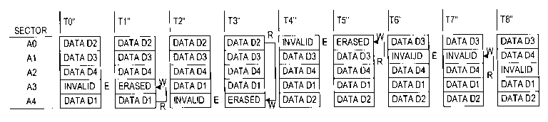
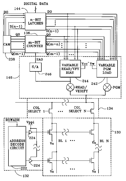
In accordance with an aspect of the invention, a multi-bit-per-cell memory includes M memory arrays with each memory array j (for j between 1 and M) storing Nj bits per memory cell. Each number Nj depends on the capability of the respective memory array j, which may vary according to variations in an integrated circuit manufacturing process. The values Nj can range between a minimum of zero, indicating the memory array is defective or otherwise not used, to Nmax, which is the maximum number of bits that the read and write circuits can provide when an array performs optimally. The memory architecture is particularly useful for mass data storage that stores blocks of data or a serial data stream at sequential memory addresses. In particular, for writing, a serial data stream of a large data file is broken into data units according to the number of bits that can be written in each memory cell. Different size data units are written in the memory arrays having different numbers of bits per memory cell. Blocks of data are partitioned into data blocks having sizes Nj×Ns where Nj is the number of bits per memory cell and Ns is the number of memory cells per sector in a memory array storing the data block. When reading the serial data or a data block, the data can be reassembled into data units having a conventional size such as 8, 16, 32, or 64 bits wide per data unit.
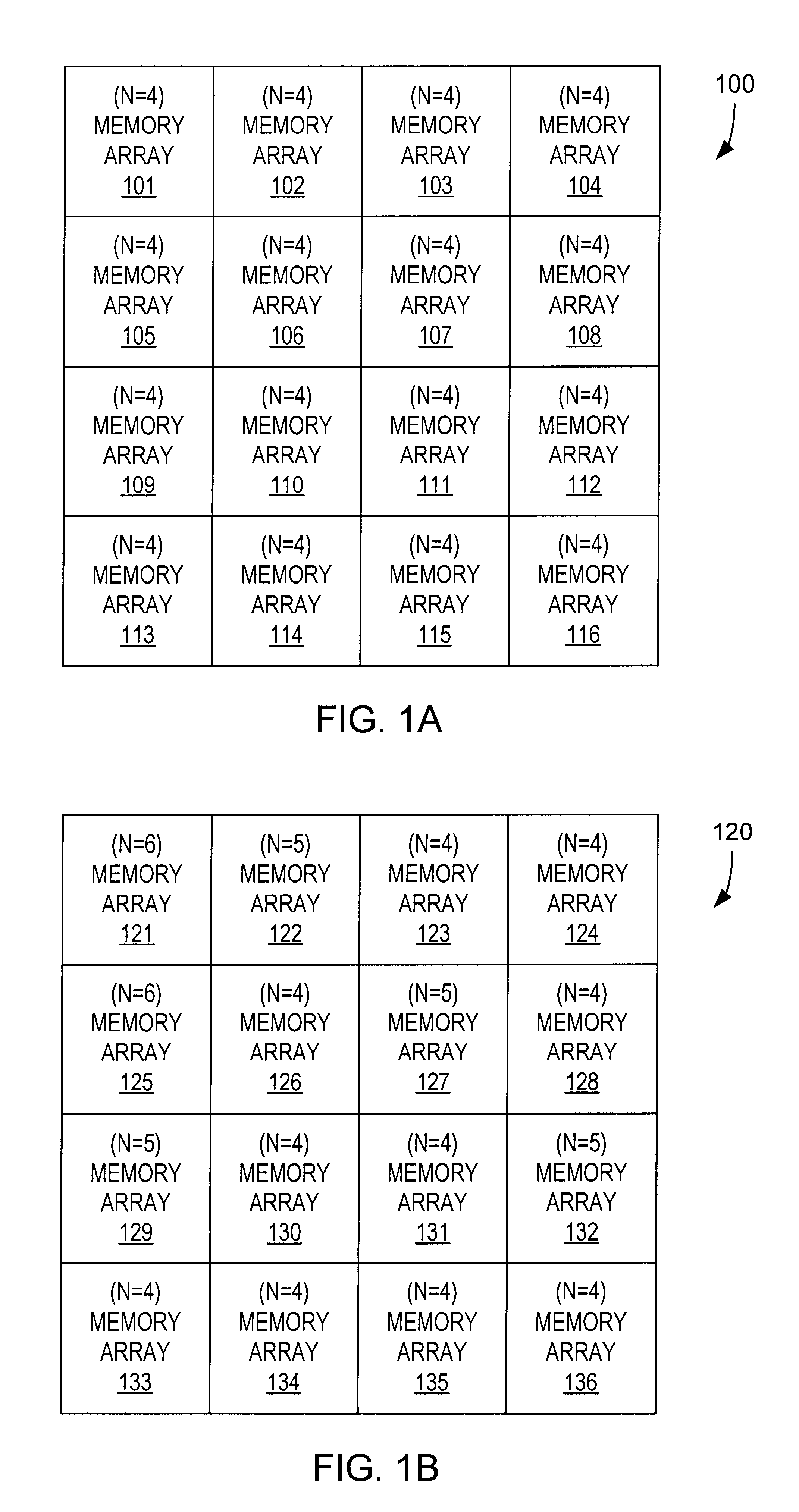
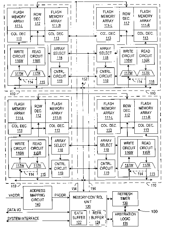
FIG. 1 is a block diagram of a memory device 100, which includes multiple memory arrays 101 through 116. Each array 101 through 116 includes a fixed number of memory cells, for example, one Meg of memory cells, and is configurable to select the number or bits stored per memory cell. Each of the arrays has associated write, read, and control circuits such as described further below.
The write circuit is designed to write a multi-bit value in a memory cell by setting a threshold voltage of the memory cell to a level corresponding to the value being written. More specifically, the write circuit accepts a multi-bit digital value having up to Nmax bits and programs a memory cell selected for a write operation to one of 2Nmax possible levels. In practice, the write circuit may lack the precision to accurately set threshold voltages at 2Nmax distinct levels. More particularly, when writing the same Nmax-bit value to two different memory cells, the two memory cells may end with different threshold voltages that the read circuit reads as different Nmax-bit values. Additionally, the memory array or specific memory cells in the array may be such that over the life of memory device 100, the threshold voltage drifts, for example, due to charge loss, charge gain, or disturbances during operation of the memory. The drift can take the threshold voltage of a memory cell from one of the 2Nmax levels to another of the levels. To avoid inaccurate writing or changes in stored values, the number Nj of bits stored per memory cell in an array generally must be smaller than Nmax.
The read circuit generates a multi-bit digital value according to the threshold voltage of a memory cell selected for reading. The multi-bit digital value includes Nmax bits, but the one or more of the least significant bits may be unreliable (and therefore unused). More specifically, one or more of the least significant bits may differ during different readings of the same cell through out the life of the memory device 100. Again, to avoid inaccuracies in read values, the number Nj of bits stored (and read) per memory cell in an array generally is smaller than Nmax.
Input and output ports of each array are configurable to select a number of input bits Nj used for a write operation or output after a read operation. Testing of an array indicates the optimal number Nj of bits per cell for the array. Generally, the number Nj is the maximum number of bits that can be accurately written and read from individual memory cells in the array. Programming of the input and output ports can be, for example, by way of laser fuses, poly fuses, or anti-fuse or using non-volatile memory elements to store the number Nj or equivalent repair information. Such fuses and similar structures are commonly employed for repair operations using redundant memory cells in conventional memory. A write circuit still uses an Nmax-bit input value, but the value being written in a memory cell only provides Nj valid bits, typically the Nj most significant bits of the Nmax-bit input value. The least significant bits can be ignored or set to a fixed value (e.g., all 0 or all 1) or to a value that maximizes the distance between the 2Nj levels required for when representing Nj-bit values. The read circuit determines an Nmax-bit read value from the threshold voltage of a selected memory cell and can ignore or truncate the least significant bits of the Nmax-bit value or perform rounding on the Nmax-bit values to generate an N-bit output value.
In an exemplary embodiment of the invention, the maximum number Nmax of input and output bits of the write and read circuits is eight, but the typical memory array in an actual integrated circuit only permits accurate writing and reading of four bits per memory cell. In the memory 100, each of memory arrays 101 to 116 performs as expected and is capable over accurately writing and reading four bits of data per memory cell. Accordingly, the total memory capacity of memory 100 is 64 Mbits (16 arrays×4 bits/cell×1 Meg cells/array).
FIG. 1B shows a memory 120 having the same design as memory 100. Memory 120 differs from memory 100 in that some memory arrays 121, 122, 125, 127, 129, and 132 perform better than expected. Other memory arrays 123, 124, 126, 127, 128, 130, 131, 133, 134, 135, and 136 in memory 120 perform as expected. In particular, memory arrays 121 and 125 are capable of writing and reading 6-bit values with the desired reliability. Memory arrays 122, 127, 129, and 132 can write and read 5-bit values with the desired reliability. Memory arrays 123, 124, 126, 127, 128, 130, 131, 133, 134, 135, and 136 can write and read 4-bit values with the desired reliability. During manufacture, a test determines the capabilities of the memory arrays 121 to 136 and programming of the I/O circuitry of memory 120 selects the numbers of bits for the arrays as given above. As a result, the total memory capacity of the memory array 120 is 72 Mbits {(2 arrays×6 bits/cell+4 arrays×5 bits/cell+10 arrays×4 bits/cell)×1 Meg cells/array}. Accordingly, a multi-bit-per-cell memory design expected to work with 4 bits per cell for a total memory capacity of 64 Mbits can actually provide memory devices with higher capacity (e.g., 72 Mbits), which presumably would command a higher market price. On the other hand, the higher capacity devices can be sold at the same price as the other available 64 Mbit devices, and provide the buyers with the option of more memory capacity.
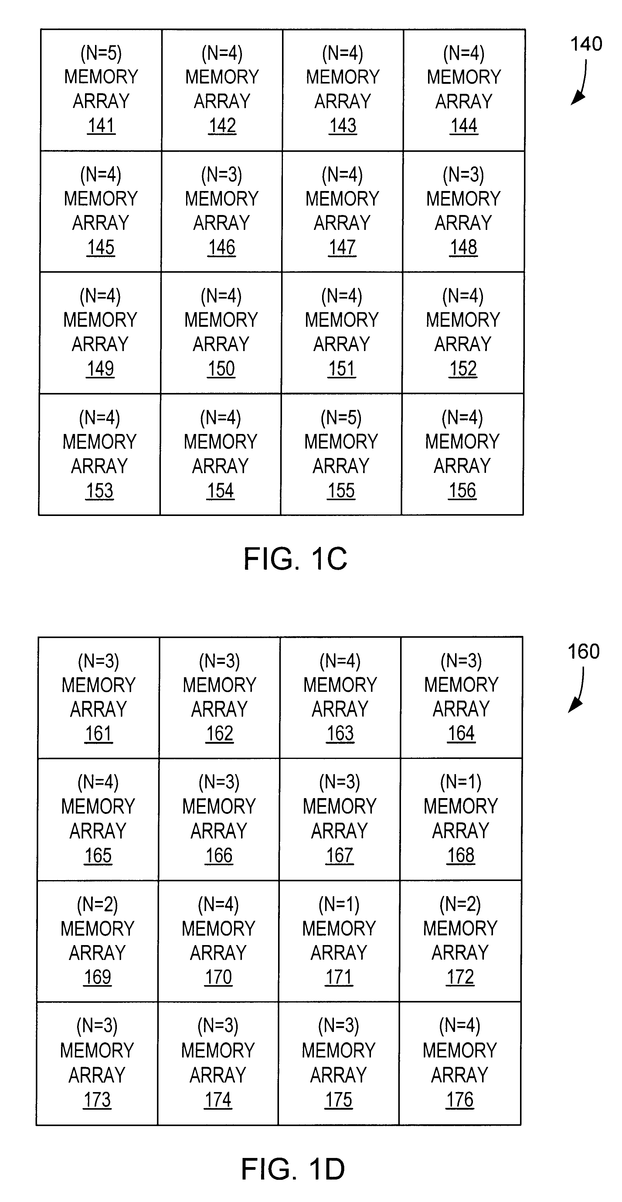
Memory arrays may also test and perform worse than expected. FIG. 1C shows a memory 140 of the same design as memories 100 and 120 of FIGS. 1A and 1B. In memory 140, arrays 141 and 155 perform better than average and can accurately write, store, and read 5 bits per memory cell. Memory arrays 142-145, 147, 149-154, and 156 perform as expected and can accurately, write, store, and read 4 bits per memory cell. However, memory arrays 146 and 148 perform worse than expected and can accurately, write, store, and read only 3 bits per memory cell. This memory would be defective and discarded in a memory architecture that demands every array to store the four bits per memory cell. However, better performing arrays of the memory 140 compensate for worse performing arrays of memory 140, and memory 140 has a total storage capacity of 64 Mbits {(2 arrays×5 bits/cell+12 arrays×4 bits/cell+2 arrays×3 bits/cell)×1 Meg cells/array}. Accordingly, the variable setting of the number of bits per memory cell allows a higher yield of operable devices having the desired density and reliability.
Even when the arrays on average perform worse than expected, the variable setting of the number of bits per cell can salvage a memory device. FIG. 1D shows a memory device 160 having the same design as memory 100 of FIG. 1, but testing indicates that arrays of memory device 160 on average perform worse than expected. In memory 160, memory arrays 163, 165, 170, and 176 perform as expected and can accurately, write, store, and read four bits per memory cell. The remaining memory arrays perform worse than expected. Memory arrays 161, 162, 164, 166, 167, 173, 174, and 175 can accurately, write, store, and read three bits per memory cell. Memory arrays 169 and 172 can accurately, write, store, and read two bits per memory cell. Memory arrays 168 and 171 can only store one bit per memory cell and effectively operate as binary memory arrays. Accordingly, the total memory capacity of memory 160 is 46 Mbits {(4 arrays×4 bits/cell+8 arrays×3 bits/cell+2 arrays×2 bits/cell+2 arrays×1 bit/cell)×1 Meg cells/array}. Accordingly, instead of discarding memory 160 as being unable to achieve the desired capacity of 64 Mbits, the memory 160 is an economically valuable memory device.
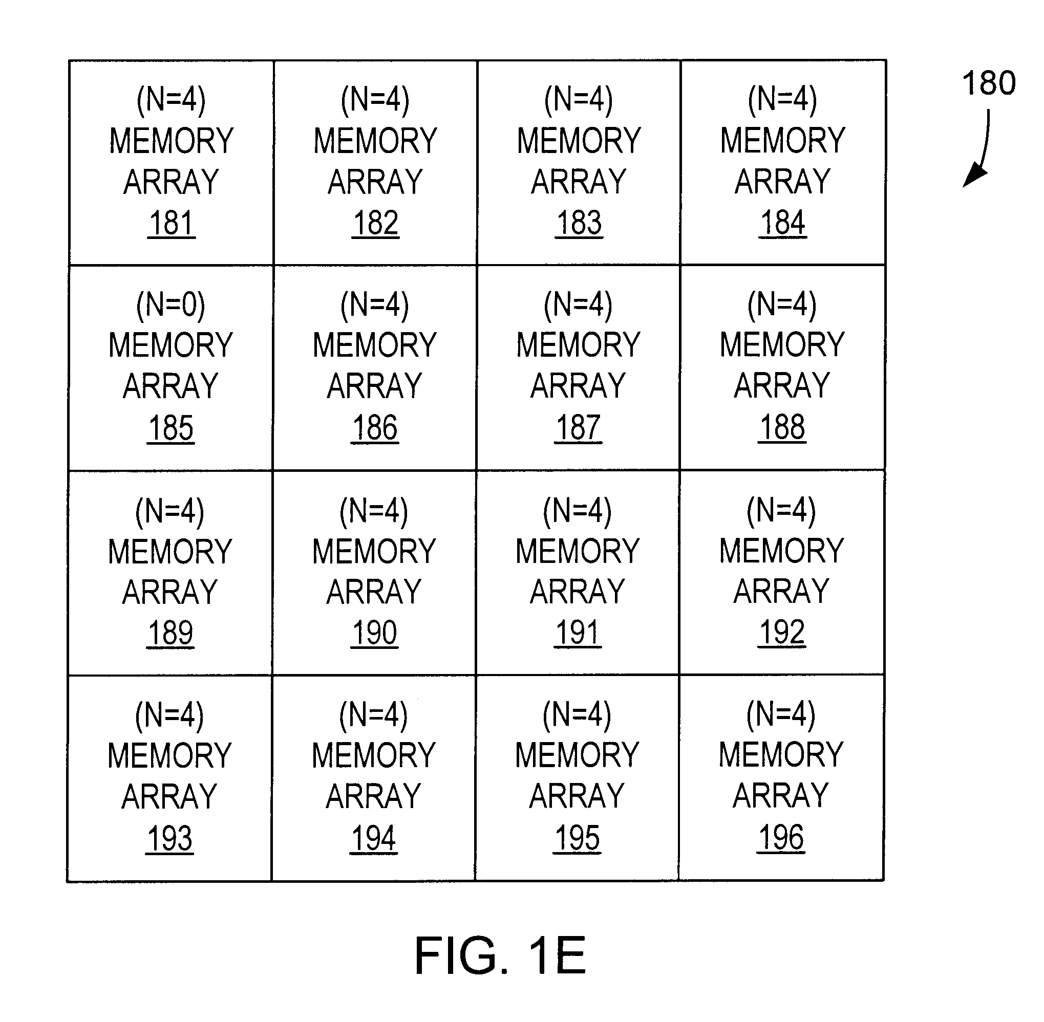
Another feature of the inventions is that a memory device can be economically valuable even if one or more arrays are defective and unable to store any data. FIG. 1E shows a memory device 180 in which one memory array 185 is defective but the other arrays 181 to 184 and 186 to 196 perform as expected and are capable of reliably writing, storing, and reading four bits per cell. The defect in memory array 185 is an unrepairable defect that makes the array unable to store any data in at least some of the addresses of the array. Memory 180 is programmed or configured to store four bits per cell in arrays 181 to 184 and 186 to 196 and no data (zero bits per cell) in array 185. Accordingly, the total capacity of memory 180 is 60 Mbits, and memory 180 is an economically valuable device instead of a device that must be discarded.
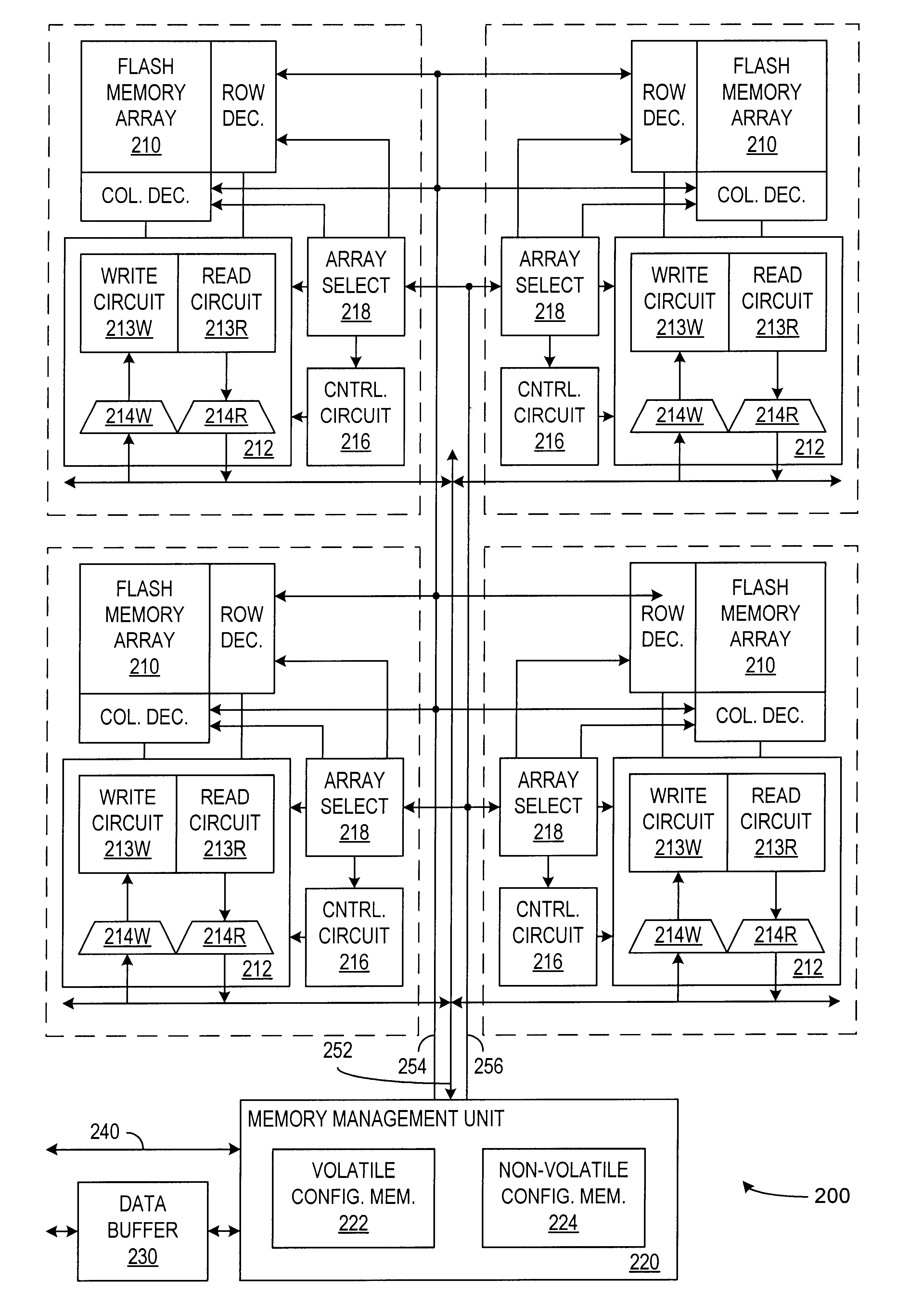
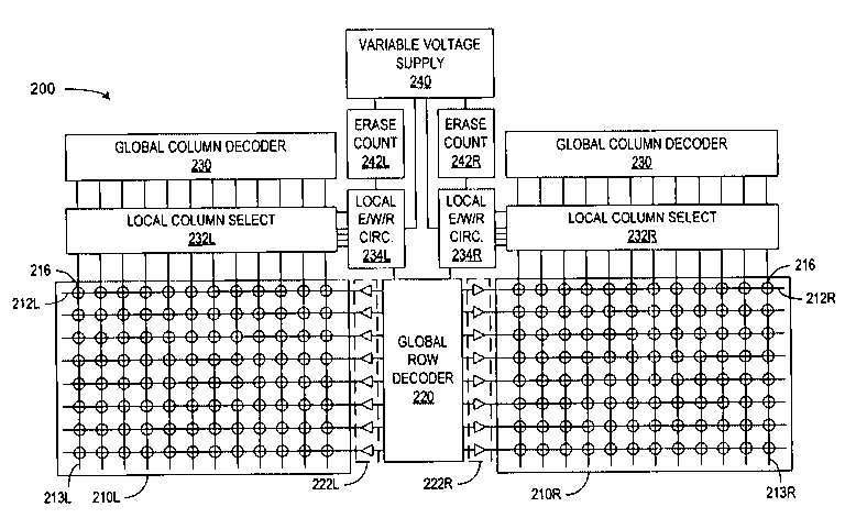
FIG. 2 is a block diagram of a multi-bit-per-cell Flash memory 200 in accordance with an embodiment of the invention. Memory 200 includes multiple memory arrays 210. Each array 210 includes rows and columns of memory cells. Each memory cell can be a conventional Flash memory cell (e.g., a floating gate transistor), an EEPROM cell, or an EPROM cell. Row lines (not shown) connect a row decoder to the control gates of memory cells in the rows of memory array 210. Column lines (not shown) connect sense amplifiers and a column decoder to drains of memory cells in the columns of memory array 210. Each array 210 is further divided into erasable sectors, and a source line connects to the sources of memory cells in an associated sector. The implementation of each array 210 and the associated row and column decoders can be conventional for multi-bit-per-cell memory. Memory arrays 210 can each consist of multiple segmented memory banks (not shown), each bank containing multiple sectors. The maximum number of memory cells on a bit-line segment depends on the maximum tolerable program disturb characteristics of the memory cells.
Also associated with each array 210 are multi-bit-per-cell write/read circuit 212, a control circuit 216, and an array selection circuit 218. A data bus 252, an address bus 254, and an array select bus 256 respectively provide data signals, address signals, and array select signals from a memory management unit 220 to the circuitry associated with arrays 210. An external control interface 240 provides control signals for operation of memory 200, and memory data buffer 230 temporarily stores data input to memory 200 or until output from memory 200.
For one embodiment of a write operation; data buffer 230 collects externally input data until data buffer 230 contains enough data to fill an entire sector of a selected memory array. The amount of data stored in a sector of a memory array j depends on the number of memory cells in the sector and the number Nj of bits stored per memory cell. Buffer 230 would normally include at least twice the capacity of a sector in a memory array that can store the maximum number Nmax of bits per memory cell. With this configuration, one portion of buffer 230 can provide the data being written to a sector, while another portion of buffer 230 continues to collect data for writing in the next selected sector. Alternatively, write operations are not required to be on a per sector basis and can begin when buffer 230 contains Nj bits of data to be written.
Memory management unit 220 generates array select signals to select one of the arrays 210 for the write operation. Address signals from the memory management unit 220 then select an erased sector in the array and a selected memory cell in the selected sector. Memory management unit 220 then retrieves an Nj-bit value from data buffer 230, where Nj is the number of bits stored per cell in the selected array. An optional volatile configuration memory 222, which contains volatile memory such as SRAM, can store the number Nj for memory management unit 220. Volatile configuration memory 222 permits configuration at power up of memory 200 and permits a user to override previous selections of the bit limits Nj. For example, at power up, values Nj can be read from non-volatile configuration memory 224 and stored in volatile configuration memory 222. Configuration memory 224 can be a ROM or an electrically programmable non-volatile memory such as Flash memory. A ROM can be programmed, for example, by cutting fuses during manufacture and testing of memory 200. Configuration memory 224 can be a separate array or may consist of memory cells scattered in the arrays 210 if configuration memory 224 uses Flash memory cells. Volatile configuration register 222 can be omitted if values Nj are read directly from non-volatile configuration memory 224 when required. Alternatively, non-volatile configuration memory 224 can be omitted, giving the user complete responsibility for setting volatile configuration memory 222.
Memory management unit 220 constructs an Nmax-bit signal for a write operation, using a corresponding Nj-bit value to be written. More particularly, the Nj-bit value provides the most significant bits of the Nmax-bit signal, and the least significant bits of the Nmax-bit signal can be selected according to a convention implemented in memory management unit 220. For example, the least significant bits can be all zero, all one, or have a value that depends on the Nj-bit value and provides a maximum separation between the Nj-bit values.
The control circuit 216 for the selected memory array 210 enables operation of the write circuitry associated with the selected array. Control circuits 216 for unselected arrays disable the write circuitry in the unselected arrays. In the embodiment, of FIG. 2, the write circuit include a converter 214W that converts the Nmax-bit signal to an analog voltage, and an analog/multi-level write circuit 213W that programs the threshold voltage of a selected memory cell to a target threshold voltage corresponding to the analog voltage. The analog/multi-level write and read circuits 212 connected to the selected array generate the programming voltages necessary to program the selected memory cell to the target threshold voltage. Analog/multi-level read and write circuits are known in the art and described, for example, in U.S. Pat. No. 5,694,356, which is hereby incorporated by reference in its entirety. The particular type of analog/multi-level write circuit used is not critical to the invention, but generally, high accuracy is desired to allow up to 2Nmax different threshold voltage levels.
When the write circuit has programmed the selected memory cell to the target threshold voltage, memory management unit 220 changes the address signal to select the next memory cell in the selected sector and retrieves the next Nj bits from data buffer 230. The write operation programs the newly selected memory cell to the threshold voltage corresponding to the next Nj-bit value. The write operation repeats until an Nj-bit value is written in the last memory cell of the selected sector or writing is otherwise complete. Memory management unit 220 then selects another sector for a write operation. If the new sector is in another array 210, memory management unit 220 changes the array select signal, reads configuration memory 222, and changes the bit limitation Nj if the number of bits stored per cell in the newly selected array differs from the number of bits per cell in the previously selected array. The writing of the sector typically begins when data buffer 230 contains enough data to fill the next data sector but alternatively can start whenever data buffer 230 contains the next Nj bits of data to be written.
For a read operation, memory management unit 220 again generates the array select signal and address signal to select an array, a sector of the selected array, and a memory cell in the selected sector. The control circuit 216 for the selected array 210 directs the associated write and read circuit 212 to read the threshold voltage of the selected memory cell. In the embodiment of FIG. 2, the read circuits include an analog/multi-level read circuit 213R and a converter 214R. Analog/multi-level read circuit 213R provides an analog signal to converter 214R representing the threshold voltage of the selected memory cell, and converter 214R outputs an Nmax-bit digital signal to the Nmax-bit wide data bus 252. Memory management unit 220 receives the Nmax-bit digital signal and extracts Nj bits of data, for example, by ignoring or truncating the least significant bits, by rounding where the least significant bits represent a fraction, or by some other more complex conversion. Data buffer 230 collects the Nj data bits from the selected memory cell. The read operation repeats for each memory cell in the selected sector so that data buffer collects the block of data originally written into the selected sector. The data can then be read out externally via the I/O interface at high speed.
The described embodiment of memory 200 can be varied in many ways. Parallel or pipelined operations can take place among memory arrays 210 or within the same memory array 210. For example, instead of writing one Nj-bit data value at a time, multiple data values having the same or different sizes can be written in parallel using one array 210 or two more arrays 210 in parallel. Alternatively, memory management unit 220 operates arrays 210 in a pipeline fashion by starting a write or read operation in an array 210 before a previously started write or read operation in that or another memory array 210 is complete. Each parallel or pipelined write operation receives an Nmax-bit value where the number Nj of bits representing actual data depends on the capabilities of the target array 210 or more specifically on the values in configuration memory 222. Each read operation similarly provides an Nmax-bit value, where Nj bits are valid and used according to the location of the memory cell read. Parallel or pipelined write and read operations provide a higher bandwidth when recording or playing back a data stream.
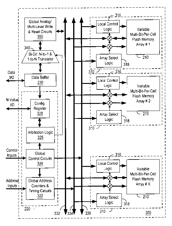
FIG. 3 illustrates an embodiment of a memory 300 that reduces overhead by sharing a converter 340 and global analog/multi-level write and read circuits 350 among multiple memory units 310, each including a memory array 210. Additionally, memory units 310 further reduce overhead by sharing global control circuits 324. Global control circuits 324 generate internal control signals that govern chip operations including erase operations, write operations, read operations, charge pump operations, stand-by mode operations, and various test operations. A typical memory can have more than fifty internal control signals. Local control logic 316 for each array 210 receives global control signals and generates appropriate local control signals that depend on whether the associated array 210 is selected.
To write a data value in a selected memory cell, converter 340 fetches Nj bits from data buffer 230 where Nj is the number of bits that are stored per cell in the selected memory array 210. A configuration register 328 stores the set of values Nj. Converter 350 converts an Nj-bit value from data buffer 230 into an analog voltage representing the value to be written in the selected memory cell. Typically, the conversion depends on the number of bits stored per memory cell in the target array so that the memory array employs the full available range of threshold voltages. Converter 350 provides the analog voltage to the global analog/multi-level write and read circuits 350.
Global analog/multi-level read and write circuits 350 generate the voltages to be applied to the selected memory cell during a write operation. More particularly, global analog/multi-level read and write circuits 350 generate row and column line voltages required for programming, which changes the threshold voltage of the selected memory cell, and row and column line voltages used to verify that the selected memory cell has reached a threshold voltage representing the data value. During a write operation, a global bus 332 carries the row and column line voltages for use by any of memory units 310.
Global address bus 334 carries address signals from global address circuits 322 in memory management unit 220 to all of memory units 310. Part of the address signal is an array select signal. The array select decoder 318 in the selected memory unit 310 recognizes the array select signal and enables use of row and column addresses from global address bus 334 and program and verify voltages from global bus 332. Row and column decoders in the selected array 210 select a memory cell according to the row and column address and apply the row and column line voltages from global bus 332 to the selected memory cell.
Similarly, during a read of a selected memory cell, global address circuits 322 generate an address signal to identify the selected memory array and the selected memory cell. The array select decoder 318 enables the row and column address to reach the row and column decoders of the selected array and connects global write and read circuits 350 to the selected array 210. Global write and read circuits 350 generate an analog signal indicating threshold voltage of the selected memory cell, and apply the signal to converter 340. Converter 340 then converts the analog signal to an Nj-bit data value where Nj is the number of bits per cell stored in the selected array as indicated in configuration register 328. As for a write operation, arbitration logic 326 reads the value Nj from configuration register 328 and controls converter 340 accordingly. Data buffer 230 collects the data values from converter 340 for output in data units of a standard size.
FIG. 3 also illustrates an embodiment of memory management unit 220 that includes global address circuits 322, global control circuits 324, arbitration logic 326, and configuration register 328. Configuration register 328 stores a set of values Nj where index j runs over a range corresponding to arrays 210 in memory 300. For normal operation, the values Nj are from non-volatile memory and loaded into configuration register 328 during start up of memory 300. The non-volatile memory can be a ROM (not shown) or part of arrays 210 in memory 300. The values Nj can be stored in ROM, for example, by setting a fuse option in response to testing memory 300. Programming erasable programmable ROM such as Flash memory with the values Nj allows possible changes in the values that will allow memory 300 to continue to operate even if one or more array 210 becomes unable to store the number of bits that initial testing indicated.
External access to configuration register 328 allows a system's CPU or controller to examine and/or select the number of bits stored per memory cell in each of the arrays. The values Nj from ROM provide a rating of the capability to store information with a particular reliability. If desired, a system can operate memory at a higher data density but a lower than normal reliability, depending on a users selection. Alternatively, based on the value Nj from ROM, the system (or the user) can selectively allocate the memory array with the most appropriate (most effective) value Nk according to the nature of the data. For example, code or program storage, which requires absolute data integrity, could be stored in a memory array 210 rated for storing a large number Nj of bits but using only Nk bits per memory cell where Nk is less than Nj to maximize data integrity. Other types of data can choose a different approach. Further, external access to configuration register 328 allows testing of the arrays by setting the value Nj for an array, writing data to that array, and reading data from that array to determine whether there are any errors.
Global address circuits 322 receive an external address indicating the memory locations or sectors to be accessed (written or read). Address circuit 322 converts the external address to an internal address identifying a first sector or first memory cell storing data corresponding to the external address. A variety of systems for the conversion between external and internal addresses are possible. For example, memory manage management unit 220 can implement a file organization or a sector access organization similar to that employed in disk drives. The external address typically corresponds to a block of data or a data unit that is stored in several memory cells. Counters in global address circuit 322 increment (or otherwise change) the internal address as required for accessing each memory cell associated with the block. The number of memory cells accessed depends on the amount of data transferred and the number Nj of bits stored per memory cell.
Although the invention has been described with reference to particular embodiments, the description is only an example of the invention's application and should not be taken as a limitation. Various adaptations and combinations of features of the embodiments disclosed are within the scope of the invention as defined by the following claims.