Skip to content

Patent drawings

Drawing 1 of 4

US 6,532,556

Drawing 1 of 4

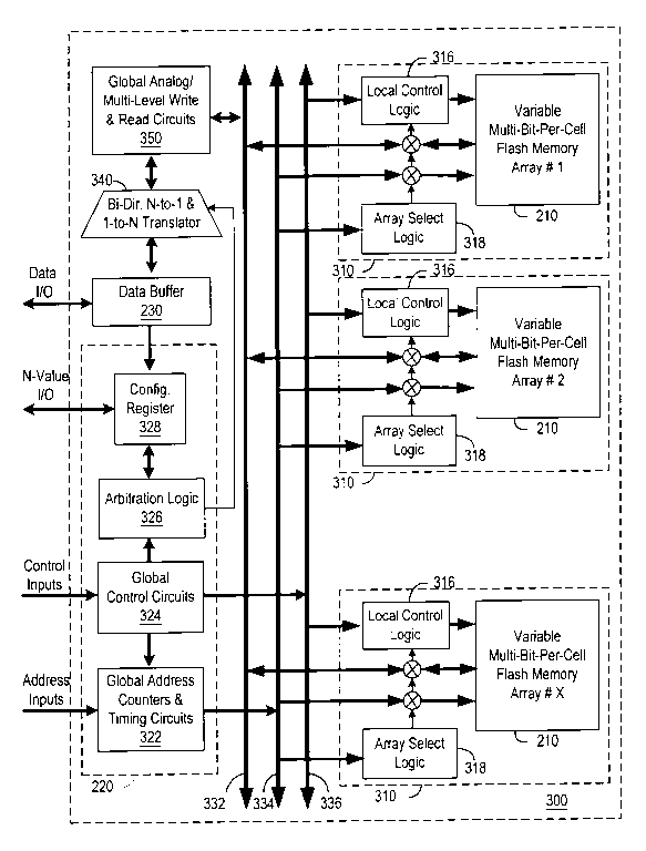
Expanded drawing 1 of 4 from US 6,532,556, Data management for multi-bit-per-cell memories
High-resolution patent drawing

US 6,532,556

Data management for multi-bit-per-cell memories

Filed
January 27, 2000
Granted
March 11, 2003
Assignee
Samsung
Previous Assignee
MLM
Inventors
Sau Ching Wong, Hock Chuen So

Abstract

A multi-bit-per-cell memory reduces the effect of defects and data errors by scrambling data bits before writing data. The scrambling prevents storage of consecutive bits in the same memory cell. When a memory cell is defective or produces an error, the bits read from the memory cell do not create consecutive bit errors that would be noticeable or uncorrectable. An error or a defect in a multi-bit memory cell causes at most scattered bit errors. Scramblers in multi-bit-per-cell memories can include 1) hardwired lines crossing between an input port and an output port, 2) programmable wiring options, 3) a linear buffer where reads from the buffer use addresses with swapped bits, or 4) a buffer array that switches between incrementing a row address first and incrementing a column address first when accessing memory cells in the buffer array.

View on Google Patents ↗
View Full PatentComplete archived record · 4 figures · 47 description paragraphs · 2 tables · 22 claims

Patent record

Source
Google Patents
Publication
US6532556B1
Application
US09/492,949
Priority
January 27, 2000
Prior art date
January 27, 2000
Publication date
March 11, 2003
Legal status
Expired - Lifetime
Original assignee
Multi Level Memory Technology
Current assignee
Samsung Electronics Co Ltd
Prior art keywords
bit, bits, scrambled, memory, data
Source retrieved
July 20, 2026

Classifications

  • GPHYSICS
  • G11INFORMATION STORAGE
  • G11CSTATIC STORES
  • G11C11/00Digital stores characterised by the use of particular electric or magnetic storage elements; Storage elements therefor
  • G11C11/56Digital stores characterised by the use of particular electric or magnetic storage elements; Storage elements therefor using storage elements with more than two stable states represented by steps, e.g. of voltage, current, phase, frequency
  • G11C11/5621Digital stores characterised by the use of particular electric or magnetic storage elements; Storage elements therefor using storage elements with more than two stable states represented by steps, e.g. of voltage, current, phase, frequency using charge storage in a floating gate
  • G11C11/5628Programming or writing circuits; Data input circuits
  • G06COMPUTING OR CALCULATING; COUNTING
  • G06FELECTRIC DIGITAL DATA PROCESSING
  • G06F12/00Accessing, addressing or allocating within memory systems or architectures
  • G06F12/14Protection against unauthorised use of memory or access to memory
  • G06F12/1408Protection against unauthorised use of memory or access to memory by using cryptography
  • G11C2211/00Indexing scheme relating to digital stores characterized by the use of particular electric or magnetic storage elements; Storage elements therefor
  • G11C2211/56Indexing scheme relating to G11C11/56 and sub-groups for features not covered by these groups
  • G11C2211/564Miscellaneous aspects
  • G11C2211/5648Multilevel memory programming, reading or erasing operations wherein the order or sequence of the operations is relevant
  • G11C29/00Checking stores for correct operation ; Subsequent repair; Testing stores during standby or offline operation

Figures

4 plates

Figure 1 of 4 from US 6,532,556, Data management for multi-bit-per-cell memories
Figure 01Full resolution ↗
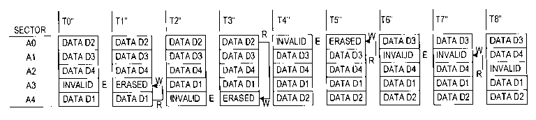
Figure 2 of 4 from US 6,532,556, Data management for multi-bit-per-cell memories
Figure 02Full resolution ↗
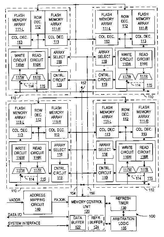
Figure 3 of 4 from US 6,532,556, Data management for multi-bit-per-cell memories
Figure 03Full resolution ↗
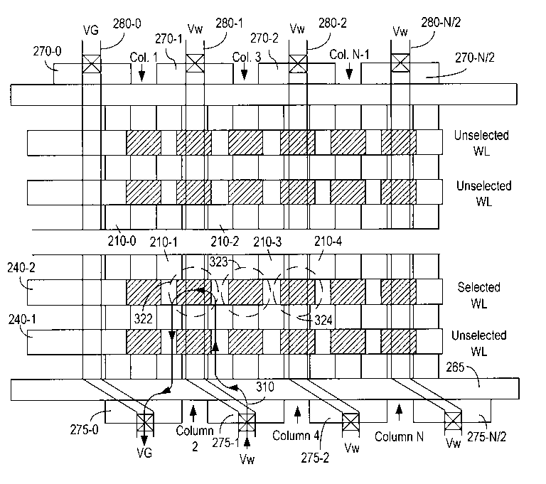
Figure 4 of 4 from US 6,532,556, Data management for multi-bit-per-cell memories
Figure 04Full resolution ↗

Description

BACKGROUND

1. Field of the Invention

This invention relates to multi-bit-per-cell memories and to data arrangements in multi-bit-per-cell memories that minimize the effect of memory errors and defects.

2. Description of Related Art

Recent developments in multi-media applications such as digital music in MP3 and AC3 formats, digital imaging for digital cameras, digital video for DV and digital camcorders, and the popularity of the internet and wireless communications have resulted in an explosive demand for cost-effective mass data storage devices with ultra high-density. Multi-bit-per-cell memories can effectively fill these needs. Multi-bit-per-cell memories use storage and retrieval techniques that provide N bits of data per memory cell and thereby increase the amount of data stored in a memory array by a factor of N when compared to binary memories. Multi-bit-per-cell Flash memories, in particular, are especially suitable for portable and battery-powered multi-media applications because Flash memories are non-volatile and provide a high-density of memory cells in an integrated circuit.

A concern when using multi-bit-per-cell memories is the accuracy of the storage and retrieval techniques. In particular, when a threshold voltage of a floating gate transistor in a memory cell represents an N-bit data value, a small error in the determination or the setting of the threshold voltage can cause a data error. Alpha particles, if not addressed properly, can also more easily create soft errors in multi-bit-per-cell memories than in conventional binary memories. Fortunately, many multi-media applications are error-tolerant or have built-in error detection and correction schemes for critical data such as the header information in an MP3 music data stream. Thus, a small number of data errors or defective memory cells may not cause a noticeable change in output quality. However, a large number of errors or multiple consecutive error bits may result in significant degradation in quality if these errors exceed the limits of the error correction technology.

Another concern is memory defects. Redundant or spare memory cells or arrays improve manufacturing yields of high-density memory ICs, particularly multi-level memories. Repair operations during fabrication of the memory ICs activate redundant memory cells of arrays in response to a test detecting one or more defective memory cells. Accordingly, before the IC memory device leaves the factory, test and repair operations can replace defective memory cells that have gross or hard defects with working redundant memory cells. Other memory cells may pass the initial testing but later fail or degrade quickly during the lifetime of the IC memory. For example, non-volatile memory cells containing floating gate transistors could have threshold voltages that change due to charge gain, charge loss, or contamination. Memory cells can also become sensitive to operating parameters such as supply voltage, temperature, and the data pattern, or endurance-related effects. The possibility of these “latent” defective memory cells often limits the use of multi-bit-per-cell memories and the maximum number of bits stored per cell because multi-bit-per-cell memories are more susceptible to latent defects.

FIG. 1 conceptually illustrates operation of a multi-bit-per-cell memory when recording an input serial data stream and playing back the serial data stream as output data. The data streams define input and output bit sequences 110 and 150. The conventional multi-bit-per-cell storage scheme groups N adjacent bits from bit sequence 110 into an N-bit value. An N-to-1 translator 120 converts the N-bit value into one of the 2N levels (e.g., a corresponding threshold voltage level) that can be written into a single memory cell 130-1 of a memory array 130. (In FIG. 1, N is four, and each translator 120 converters a 4-bit value into one of 16 levels for storage in a memory cell.) The next N data bits from the serial data bit stream are grouped and written into a physically adjacent memory cell 130-2, typically in the same row or column as the previously accessed memory cell.

During the read (or playback) operation, the level stored in each memory cell is read, and a 1-to-N translator converts the read level back into the N adjacent bits. Finally, assembly of all of the bits read from adjacent memory cells constructs the bit sequence 150.

A multi-level memory having two translators 120 and 140 for each memory cell has too much overhead to be practical. FIG. 2 illustrates a more typical multi-bit-per-cell memory 200 including a memory array 210 with one N-to-1 translator 220 and one 1-to-N translator 230 that are multiplexed or shared among all the memory cells. A multi-level write circuit 225 programs a memory cell in array 210 according to the level from N-to-1 translator 220, and a multi-level read circuit 235 reads a memory cell to provide a read level to 1-to-N translator 230. A shift register 250 and a multiplexing circuit 240 control partitioning of an input serial data stream of M-bits into N-bit data units for N-to-1 translator 220 and assembling of N-bit data units from 1-to-N translator 230 to form the output serial data stream.

In the conventional scheme, any single memory cell failure can potentially affect N adjacent bits of the serial data stream. In particular, a slight shift in the read or written threshold voltage of a memory cell can corrupt all N adjacent data bits stored in the memory cell. For example, conventional binary coding of threshold voltage levels has adjacent data values 011 . . . 11b and 100 . . . 00b correspond to adjacent threshold voltage levels. A shift from one threshold voltage level to the adjacent threshold voltage level can changes all N bits (e.g., from 011 . . . 11b to 100 . . . 00b). If these N adjacent data bits all come from the same audio sample or the same pixel in an image, the error may cause a significant and noticeable distortion in the output signal (audio or image) upon playback.

U.S. Pat. No. 5,909,449, entitled “Multi-Bit-Per-Cell Non-Volatile Memory with Error Detection and Correction,” which is hereby incorporated by reference in its entirety, describes Gray coding of threshold voltages to prevent more than a single bit error when a memory cell threshold voltage shifts from one level to an adjacent level. The Gray coding method is subject to multiple consecutive bit errors if a single memory cell fails in a more significant way than a single level shift. Accordingly, further methods for minimizing the effects of data errors in multi-level memories are sought.

SUMMARY

In accordance with an aspect of the invention, a data management method minimizes the effect that defective memory cells have on the quality of the data stored in multi-bit-per-cell memories.

A data management method in accordance with one embodiment of the invention mixes or scrambles a bit sequence from an input serial data stream before storage. The mixing or scrambling separates consecutive bits from each other. Consecutive bits are stored in different multi-level memory cells that are preferably physically spaced apart from each other in a memory array. Accordingly, any single memory cell failure or adjacent memory cell failures (such as one or more cells along a column or along a row) caused by threshold voltage drift, localized defects, endurance-related failures or soft errors, does not cause a long string of consecutive bit errors. The mixing of data bits spreads the effect of any single memory cell failure among data coming from, for example, different audio samples (at different times or different frequencies) or different pixels (for image or video) and typically makes the defects much less noticeable or easier to correct.

One embodiment of the invention is a multi-bit-per-cell memory that includes a storage array, a scrambler, and a write circuit. Each memory cell in the storage array stores N bits of information. The scrambler receives data including a group of M data bits and generates a set of scrambled N-bit values from the group of M data bits. Each scrambled N-bit value has bits in an order that differs from the bit order in the group. The write circuit receives the set of scrambled N-bit values from the scrambler and writes each scrambled N-bit value in an associated memory cell. In one embodiment, the memory further includes: a read circuit and a descrambler, but the descrambler can be implemented using the elements of the scrambler. The descrambler receives a set of N-bit values read from associated memory cells of the storage array and mixes bits from the N-bit values to reconstruct a group of M data bits.

Exemplary implementations of the scrambler include: a data input port hardwired to scramble data bits that are output from an output port; a linear buffer that outputs data bits in an order that differs from the order in which data was stored; and a buffer array with an address control circuit operable in a first mode that increments a row address for each bit accessed in the buffer array and a second mode that increments a column address for each bit accessed in the buffer array. With the buffer array, the scrambler provides a scrambled N-bit value by: sequentially writing bits from the group into the buffer array while operating in one of the first and second modes; changing mode; and reading N bits from the buffer array. For reading and data output, the scrambler provides output data by: sequentially writing bits from the read circuit into the buffer array while operating in one of the first and second modes; changing mode; and reading the output data from the buffer array.

In accordance with another embodiment of the invention, a method for writing or arranging data in a multi-bit-per-cell memory, includes scrambling data bits from an input serial data stream to create a scrambled data stream; partitioning the scrambled data stream into a set of N-bit values; and writing each N-bit value in a corresponding memory cell. Consecutive bits from the input serial data stream are not consecutive in the scrambled data stream so that a data error or defect in a single memory cell does not cause a string of N consecutive data errors. Operating the memory further includes reading a set of N-bit values from a set of the memory cells, and mixing bits from different N-bit values to generate output data. Circuitry inside an integrated circuit memory device such as the multi-bit-per-cell memories described herein can perform the scrambling, partitioning, writing, reading, and mixing.

BRIEF DESCRIPTION OF THE DRAWINGS

FIG. 1 illustrates conventional processes for recording or playing a serial data stream in a multi-bit-per-cell memory.

FIG. 2 is a block diagram of a conventional multi-level memory.

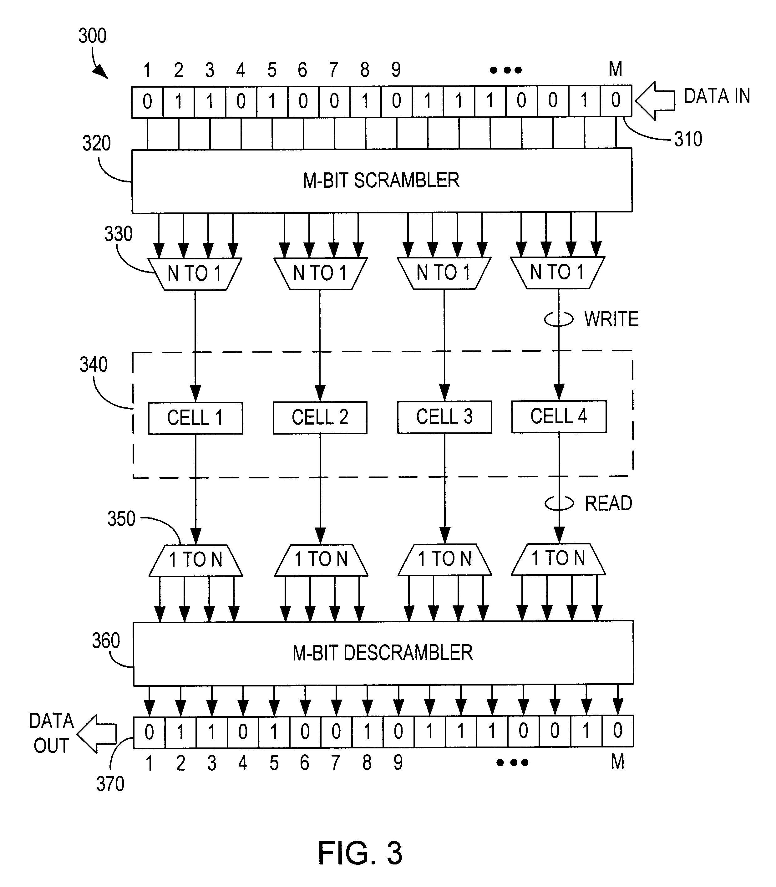
FIG. 3 illustrates a multi-bit-per-cell memory in accordance with an embodiment of the invention that scrambles a bit sequence for writing in memory cells and reconstructs the bits sequence when reading from the memory cells.

FIG. 4A illustrates a multi-bit-per-cell memory including a hardwired scrambler in accordance with an embodiment of the invention.

FIG. 4B shows a portion of a programmable scrambler that can replace the hardwired scrambler and descrambler of FIG. 4A.

FIG. 5 illustrates a multi-bit-per-cell memory in which a scrambler includes a linear buffer in accordance with an embodiment of the invention.

FIG. 6 illustrates a multi-bit-per-cell memory in which a scrambler includes a buffer array in accordance with an embodiment of the invention.

Use of the same reference symbols in different figures indicates similar or identical items.

DETAILED DESCRIPTION

In accordance with an aspect of the invention, a multi-bit-per-cell memory includes a data management circuit that selects non-consecutive bits from a serial data stream for storage in a memory cell. In one embodiment of an N-bit-per-cell memory, N consecutive bits are stored in N different memory cells, and X bits of the bit sequence are between any pair of bits stored in the same memory cell. The integer X is typically greater than or equal to N-1 and can be selected according to the type of data being stored in the multi-bit memory. In particular, X can be selected according to the size of data units in a serial data stream to avoid multiple bit errors in the same data unit of the data stream.

FIG. 3 illustrates a multi-bit-per-cell memory 300 in accordance with an embodiment of the invention. Memory 300 employs a data management process that partitions an input bit sequence from an input serial data stream into groups of M bits. M is an integer multiple of N, and N is the number of bits stored per cell in a storage array 340. A register 310 stores an M-bit group from the input serial data stream. An M-bit scrambler 320 mixes or scrambles the bits in each original M-bit group from register 310 to generate a scrambled M-bit group. The scrambled M-bit group includes (M/N) scrambled N-bit values that are input to a write circuit including translators 330. Translators 330 translate each scrambled N-bit value into one of the 2N levels for writing into a corresponding one of the multi-level memory cells in array 340. Each translator 330 can perform any type of mapping from the N-bit values to the 2N levels but preferably performs a linear translation or a Gray coding of the N-bit value.

For a multi-bit-per-cell Flash memory, the 2N levels from translators 330 correspond to 2N different target threshold voltage to which write circuitry can program a memory cell. A write operation for an M-bit group programs the threshold voltages of (M/N) memory cells to the levels associated with the respective N-bit scrambled values. The N-bit write operations can be performed in parallel, pipelined, or sequentially. For a sequential write operation, the write circuitry writes one scrambled N-bit value at a time, and only one translator 330 is required. Parallel or pipelined write operations can provide faster performance and higher bandwidth but require additional circuitry and consequentially additional circuit area and cost. Write and read circuits for multi-bit-per-cell memories are known in the art and described, for example, in U.S. Pat. No. 6,038,166, entitled “High Resolution Multi-Bit-Per-Cell Memory,” which is hereby incorporated by reference in its entirety. U.S. Pat. No. 5,680,341, entitled “Pipelined Record and Playback for Analog Non-Volatile Memory”; U.S. Pat. No. 5,969,986, entitled “High-Bandwidth Read and Write Architecture for Non-Volatile Memories”; and U.S. Pat. No. 6,278,633, entitled “High Bandwidth Flash Memory that Selects Programming Parameters According to Measurements of Previous Programming Operations” describe suitable pipelined memory architectures and are also incorporated by reference in their entirety.

Upon playback of the M-bit group, the levels of the M/N cells from array 340 are read out, and translators 350 translate each level read back into an N-bit scrambled value. An M-bit descrambler 360 receives (M/N) scrambled N-bit values as read from memory cells 340-1 to 340-(M/N) and then re-mixes or unscrambles the scrambled M bit group to obtain the original M-bit data group. The M-bit descrambler 360 writes the original M-bit data group in a register 370 for output from memory 300 in the data units of the data stream.

There are many ways to mix the M bits of each group. For example, scrambler 320 can be hardwired on a chip or can be user-programmable to rearrange the M bits in a user-selected manner. Descrambler 370 performs the inverse of the mapping that scrambler 320 performs and can be hardwired or user-programmable.

In one embodiment, scrambler 320 implements an arbitrary mapping between an original M-bit group and a scrambled M-bit group. Hardwired connections between an input port for the original M-bit group and an output port for the scrambled M-bit group define the mapping. The connections between the input and output ports can also be programmable using routing circuitry making connections selected by a configuration register.

In another embodiment of the invention, scrambler 320 implements one-dimensional mixing according to an address defining the position of each bit in the original M-bit group. For example, if M is equal to 2k, the k address bits that decode the M bits in a binary sequence may be rearranged to scramble the binary sequence. For example, each bit in the original M-bit group has an address according to the bit's position in the original M-bit group, but the bit's position in the scrambled M-bit group has address bits swapped. Table 1 shows a mapping that interchanges address bits 0 and 2.

TABLE 1

Alternatively, a two-dimensional address mixing scheme temporarily stores an M-bit group in a buffer array having binary memory cells in x rows and y columns, i.e., an x-by-y-bit buffer array. In this case, M is the product of x and y (M=x*y). In one scheme, when sequentially writing bits from the input bit sequence to the buffer array, the row address is cycled first (i.e., incremented for each bit written). After writing fills a column of the array, the column address is incremented and writing begins in the next column. Table 2 shows the resulting storage of data bits in the buffer memory array.

TABLE 2
Column 1Column 2. . .Column y
Row
1Data Bit 1Data Bit (x + 1). . .Data Bit (x(y − 1) + 1)
Row 2Data Bit 2Data Bit (x + 2). . .Data Bit (x(y − 1) + 2)
.... . ..
.... . ..
.... . ..
Row xData Bit xData Bit (2x). . .Data Bit (x * y)

When reading from the array, the column address is cycled first. After reading a row, the row address is incremented and reading begins in the next row. Writing and reading the bits in the described orders provides a scrambled M-bit sequence DB1, DB(x+1), DB(2x+1), . . . , DBx, DB2x, . . . , DB(x*y) from the original bit sequence DB1, DB2, . . . , DBx, DB(x+1), DB(x+2), . . . , DB(x*y). Bits that are adjacent in the original input sequence are separated by y−1 intervening bits in the scrambled input sequence.

Descrambler 360 can reverse or descramble the scrambling by cycling the column address first while writing the scrambled bit sequence into an x-by-y buffer array and cycling row address first during reading from the buffer array. Alternatively, scrambler 320 scrambles by cycling the column address first while writing the original bit sequence into the buffer array and cycling row address first during reading from the buffer memory array; and descrambler 360 descrambles by cycling the row address first while writing the scrambled bit sequence into the buffer array and cycling column address first during reading from the buffer array.

Use of the above described scrambling reduces the effect that data errors have on multimedia data. For example, a MP3 music data stream includes coded spectral data information for 32 subbands (frequencies). The 2-dimensional buffer memory array described above can temporarily store data from different subbands in different columns of the buffer array. When data are read out of the buffer memory array, data bits from one row, thus coming from different subbands, are grouped together before writing into the memory cells in the multi-level memory array. Accordingly, an error in one memory cell affects at most one bit in each of N subbands, instead of changing N bits in a single subband value. Generally, the single bit errors in several subbands have a less noticeable effect than does an N-bit error in a single subband.

FIG. 4A illustrates a multi-level memory 400 with a hardwired scrambler 420 and a hardwired descrambler 460 in accordance with an embodiment of the invention. Multi-level memory 400 stores four bits of data per memory cell (N=4) and partitions input data into 16-bit groups (M=16) for scrambling. A shift register 410 receives a 16-bit data group for storage in a memory array 340. Scrambler 420 has an input port coupled to register 410 and an output port coupled to a write circuit 430. For a write operation, hardwired scrambler 430 mixes the 16 bits from shift register 410 and provides four 4-bit scrambled values to write circuit 430. Hardwiring in scrambler 420 can implement any mapping of the input port bits to the output port bits. In memory 400, the first scrambled 4-bit value includes bits 1, 5, 9, and 13 from shift register 410, the second scrambled 4-bit value includes bits 2, 6, 10, and 14 from shift register 410, the third scrambled 4-bit value includes bits 3, 7, 11, and 15 from shift register 410, and the fourth scrambled 4-bit value includes bits 4, 8, 12, and 16 from shift register 410. This happens to be equivalent to the one-dimensional scrambling described above where address bits 0 and 2 of the original 4-bit address are unchanged but address bits 1 and 3 are swapped.

Write circuit 430 writes the four scrambled values in four separate memory cells, for example, at four consecutive addresses in the memory array 340. Write circuit 430 can be any type of write circuit capable of writing a 4-bit value in a memory cell. In particular, write circuit 430 can be a conventional write circuit for a multi-bit-per-cell Flash memory that writes a 4-bit value in a memory cell by programming a threshold voltage of the memory cell to a target level associated with the 4-bit value. Such write circuits are well known in the art and can be implemented to write the four 4-bit values simultaneously (in parallel or pipelined) or sequentially. After writing the four 4-bit scrambled values, the next 16 bits in the serial data stream are loaded into shift register 410, and write circuit 430 writes the next set of four scrambled values in the next set of four memory cells of array 340.

A playback operation reads a series of memory cells and reconstructs a serial data stream from the values read. In memory 400, a read circuit 450 reads four memory cells and provides four 4-bit values to descrambler 460. In the exemplary embodiment of the invention, reading of a memory cell identifies a 4-bit digital value corresponding to the threshold voltage of the memory cell being read. A variety of read circuits capable of reading multiple bits from a memory cell are known in the art. Such read circuits can perform parallel, pipelined, or sequential operations to determine four read values. Descrambler 460 receives the four read digital values and directs individual bits for storage in specific bit locations in shift register 410. The descrambler 460 undoes the scrambling of scrambler 430. For example, the four bits from the first scrambled value are stored in bit locations 1, 5, 9, and 13 respectively in shift register 410. Shift register 410 then provides the output data in the correct order, which is the same order as in the input data stream. The record and playback operations of memory 400 can share a single shift register 410 since record and playback operations are typically not conducted simultaneously. Alternatively, memory 400 can include separate input and output shift registers to reduce the multiplexing circuits required between the shift register 410 and the read or write circuits.

Hardwired scrambler 420 and descrambler 460 are adaptable to wide variation in the connections between input and output ports. Further, scrambler 420 and descrambler 460 can include wiring options with a value in a configuration register selecting which wiring option conducts signals between the input and output ports. Such wiring options can be based on cross-point switches similar to configuration of a field programmable gate array.

FIG. 4B shows a programmable scrambler 425 that can replace the hardwired scrambler 420 of FIG. 4A. For each M output bits, scrambler 470 includes a set of transfer gates 470 and a configuration register 480. Configuration register 480 is an SRAM-based memory array that is configured during power up, by loading data from non-volatile memory (not shown) such as on-chip flash memory or an external Flash memory or EEPROM into configuration register 480. Each configuration register 480 turns on a single pass gate from the associated set 470 to select which bit from the input register 410 provides the output bit corresponding to that configuration register. The descrambler 460 can be similarly implemented with a full programmable scrambler such as scrambler 425, but the programming of the descrambler must be such that the descrambler undoes the bit mapping of the scrambler. Thus, the scrambling and corresponding descrambling can be user programmable to select scrambling for the type of data stream being stored. For example, scrambling can be tailored for the sizes of data units in the data stream.

FIG. 5 is a block diagram of a multi-bit-per-cell memory 500 implementing one-dimensional scrambling and descrambling for writing and reading a serial data stream. Memory 500 includes a linear buffer or input/output register 510 for data being written to or read from a multi-bit-per-cell storage array 540. An address control circuit 520 controls the order in which data bits are written to or read from I/O register 510. In particular, to record a serial data stream, input data bits are sequentially stored in I/O register 510 in a manner similar to a shift register so that M bits of data are in register 510 with the same order as in the serial data stream. Address control circuit 520 controls the order in which bits from I/O register 510 are passed to a write register 515. For example, instead of sequentially outputting bits from register 510 to register 515 according to a sequential counter, address control circuit 520 can swap address bits from a counter when designating which bit to output to register 515. When register 515 contains N bits scrambled according to the address signal from address control circuit 520, a translator 530 and a write circuit 535 write the scrambled N-bit value in a memory cell of storage array 540.

To read or play back the serial data stream, a read circuit 550 reads memory cells of storage array 540 in the order in which the memory cells were written. The read circuit 550. and a translator 555 provide the N-bit values read from storage array 540 to a read register 560. Read register 560 sequentially outputs bits to I/O register 510, and address control circuit 520 provides the addresses indicating where each bit is written. In particular, the address for writing from read register 560 reverses the address bit swapping used when writing from I/O register 510 to write register 515. The address bit swapping like the hardwired scrambling can be made user programmable through a configuration register (not shown).

FIG. 6 is a block diagram of a multi-bit-per-cell memory 600 implementing two-dimensional scrambling and descrambling for writing and reading a serial data stream. Memory 600 includes a buffer memory array 620 and a multi-bit-per-cell storage array 640. Buffer array 620 is a conventional buffer including binary volatile memory cells (e.g., SRAM or DRAM cells) arranged in six rows and six columns. In FIG. 6, the memory cells in buffer 620 are numbered 1 through 36 indicating the order in which sequentially received data bits are written to buffer 620 when received from a buffer register 610 for recording in storage array 640. A buffer address control circuit 628 generates row and column address signals for a buffer row decoder and drivers 622 and a buffer column decoder, drivers, and sense circuits 624, respectively during access of buffer array 620.

For recording of a serial data stream, buffer input register 610 receives the data stream from outside memory 600 and passes individual bits to buffer column decoder drivers 624 for storage in buffer array 620. Buffer address control 628 increments the row address for each bit written in buffer array 620 and increments the column address after writing a data bit to the last memory cell in a column. This process writes 36 bits to memory cells 1 to 36 in order. After writing the 36 bits to array 620, buffer address control 628 generates address bits for reading bits from buffer array 620 and storing the bits in a buffer output register 670. For this read operation, buffer address control 628 increments the column address for each bit read from buffer array 620 and increments the row address after reading a data bit from the last memory cell in a row.

Buffer output register 670 receives and collects the bits read from buffer array 620 and provides 4-bit scrambled values to a translator 630 for storage in a memory cell in storage array 640. For example, the first 4-bit scrambled value includes bits 1, 7, 13, and 19, and the second 4-bit scrambled value includes bits 25, 31, 2, and 8. For 36 bits stored in buffer array 620, translator 630 receives nine scrambled 4-bit values for writing in storage array 640. A write circuit 635 sequentially, in parallel, or in pipelined manner writes each scrambled 4-bit value a corresponding memory cell. During this time, the buffer input register 610 holds any new input data until the new data can be written in buffer array 620 without interfering with the transfers from buffer array 620 to register 670. The process subsequently continues with writing 36 bits to buffer array 620, reading scrambled values from buffer array 620, and writing the scrambled values in storage array 640.

To retrieve or playback a serial data stream from storage array 640, a read circuit 650 reads storage cells of array 640 in the order in which the storage cells where written. For each storage cell read, a translator 655 converts a level read from the cell into a scrambled 4-bit value and stores that value in buffer input register 610. Buffer address control 628 generates address signal for writing the read bits in buffer array 620 starting at memory cell 1. For this write operation, buffer address control 628 increments the column address for each bit written to buffer array 620 and increments the row address after writing a bit to the last memory cell in a column. After writing 36 bits that result from reading nine storage cells, buffer address control 628 controls reading of data from buffer array 620 into buffer output register 670 for output from memory 600. For this operation, buffer address control 628 increments the row address for each bit read from buffer array 620 and increments the column address after reading a data bit from the last memory cell in a column.

Although the invention has been described with reference to particular embodiments, the description is only an example of the invention's application and should not be taken as a limitation. Various adaptations and combinations of features of the embodiments disclosed are within the scope of the invention as defined by the following claims.

Claims (22)

  1. A multi-bit-per-cell memory comprising: an array of memory cells wherein each memory cell stores N bits of information; a scrambler connected to receive a group of M data bits and provide a set of scrambled N-bit values containing bits from the group, wherein M is an integer greater than N, and bits in each scrambled N-bit value have an order that differs from an order in the group; and a write circuit coupled to the scrambler and the array, wherein the write circuit writes each scrambled N-bit value from the scrambler into a memory cell associated with the scrambled N-bit value.
  2. The memory of claim 1, further comprising: a read circuit coupled to read the memory cells of the array; and a descrambler coupled to the read circuit, wherein the descrambler receives a set of N-bit values read from associated memory cells of the array and mixes bits from the N-bit values to reconstruct a group of M data bits.
  3. The memory of claim 1, wherein the scrambler is hardwired to receive M bits in an order according to the group, mix the M bits to provide a scrambled M-bit group, and partition the scrambled M-bit group into the scrambled N-bit groups.
  4. The memory of claim 3, wherein the scrambler comprises: an input port that receives the M bits in the order according to the group; an output port that provides the scrambled M-bit group; and connections between the input port and the output port that scramble the order of the bits of the M-bit group.
  5. The memory of claim 1, wherein the scrambler is programmable to select a mapping according to which the scramble maps the M-bit group to a scrambled M-bit group that is partitioned into the scrambled N-bit groups.
  6. The memory of claim 1, wherein: each bit in the group has a multi-bit address defining a position of the bit in the group; and the scrambler receives M bits of the group, creates a scrambled M-bit group by reordering each bit of the group according to a new address that results from swapping bits in the multi-bit address, and partitions the scrambled M-bit group into the scrambled N-bit groups.
  7. The memory of claim 1, wherein the scrambler comprises: a buffer array; and an address control circuit for operation of the buffer array, the address control circuit being operable in a first mode that increments a row address for each bit accessed in the buffer array and a second mode that increments a column address for each bit accessed in the buffer array, wherein the scrambler provides a scrambled N-bit value by: sequentially writing bits from the group into the buffer array while operating in one of the first and second modes; changing mode; and then reading N bits from the buffer array.
  8. The memory of claim 7, further comprising a read circuit coupled to read the memory cells of the array, wherein the scrambler provides output data by: sequentially writing bits from the read circuit into the buffer array while operating in one of the first and second modes; changing mode; and then reading the output data from the buffer array.
  9. The multi-bit-per-cell memory of claim 1, wherein the scrambled N-bit values are such that no pair of consecutive bits in the group of M data bits are written into the same memory cell.
  10. The multi-bit-per-cell memory of claim 1, wherein the group of M data bits contains X-bit data units, and the scrambled N-bit values are such that no two bits from the same X-bit data unit are in the same scrambled N-bit value.
  11. The multi-bit-per-cell memory of claim 1, wherein the scrambled N-bit values are such that each set of N bits that are consecutive in the group of M data bits is spread over multiple memory cells when written in the array.
  12. A method for writing data to a multi-bit-per-cell memory, comprising: scrambling data bits from a data stream to create a scrambled data stream, wherein the data stream contains X-bit data values with X being greater than 1; partitioning the scrambled data stream into a set of N-bit values, wherein N is greater than 1; and writing each N-bit value in a corresponding memory cell, wherein the scrambling is such that for each X-bit data value in the data stream, no two bits from the X-bit data value are written in the same memory cell.
  13. The method of claim 12, wherein circuitry inside an integrated circuit memory device performs the scrambling, partitioning, and writing.
  14. The method of claim 12, further comprising: reading a set of read N-bit values from a set of the memory cells; and mixing bits from different read N-bit values to generate output data.
  15. The method of claim 14, wherein circuitry inside an integrated circuit memory device performs the scrambling, partitioning, writing, reading, and mixing.
  16. The method of claim 12, wherein scrambling comprises receiving M bits at an input port that is hardwired to an output port, wherein hardwiring causes an order of bits along the output port to differ from an order of bits along the input port.
  17. The method of claim 12, wherein: each bit in an M-bit group from the data stream has a multi-bit address defining a position of the bit in the data stream; and scrambling comprises creating a scrambled M-bit group by ordering each bit according to a new address that results from swapping bits in the multi-bit address defining the position of the bit in the data stream.
  18. The method of claim 12, wherein scrambling comprises: sequentially writing bits from the data stream into a buffer while operating in the buffer in a first mode; and reading bits from the buffer array while operating in the buffer in a second mode, wherein one of the first and second modes increments a row address for each bit accessed in the buffer, and another of the first and second modes increments a column address for each bit accessed in the buffer.
  19. A multi-bit-per-cell memory comprising: an array of memory cells wherein each memory cell stores N bits of data, wherein N is greater than 1; a scrambler connected to scramble bits of an input M-bit data group to generate a scrambled M-bit group, wherein the scrambled M-bit data group includes multiple scrambled N-bit values; and a write circuit coupled to the scrambler and the array, wherein the write circuit writes each scrambled N-bit value into a different one of the memory cells of the array.
  20. The multi-bit-per-cell memory of claim 19, wherein the scrambled N-bit values are such that no pair of bits that are consecutive in the input M data group are written into the same memory cell.
  21. The multi-bit-per-cell memory of claim 19, wherein the input M-bit data group contains X-bit data units, and the scrambled N-bit values are such that no two bits from the same X-bit data unit are in the same scrambled N-bit value.
  22. The multi-bit-per-cell memory of claim 19, wherein the scrambled N-bit values are such that storage of each set of N bits that are consecutive in the input M-bit data group is spread over multiple memory cells in the array.

Publications

Related applications (3)

  1. US09/492,949

    Priority application

  2. US09/492,949

    Claims priority

  3. US09/492,949

    Patent family

Record timeline

  1. Application filed by Multi Level Memory Technology

  2. Priority to US09/492,949

  3. Assigned to MULTI LEVEL TECHNOLOGY

  4. Assigned to MULTI LEVEL MEMORY TECHNOLOGY

  5. Application granted

  6. Publication of US6532556B1

  7. Assigned to MULTI LEVEL MEMORY TECHNOLOGY (NEVADA)

  8. Assigned to INTERNATIONAL DEVELOPMENT AND LICENSING

  9. Assigned to SAMSUNG ELECTRONICS CO., LTD.

  10. Anticipated expiration

  11. Expired - LifetimeCurrent

Legal events

  1. AS

    Assignment

    Owner name: MULTI LEVEL TECHNOLOGY, CALIFORNIA

    Free format text: ASSIGNMENT OF ASSIGNORS INTEREST;ASSIGNORS:WONG, SAU CHING;SO, HOCK CHUEN;REEL/FRAME:011738/0616;SIGNING DATES FROM 20010315 TO 20010327

  2. AS

    Assignment

    Owner name: MULTI LEVEL MEMORY TECHNOLOGY, CALIFORNIA

    Free format text: CORRECTIVE ASSIGNMENT TO CORRECT THE ASSIGNEE'S NAME PREVIOUSLY RECORDED ON REEL 11738, FRAME 616.;ASSIGNORS:WONG, SAU CHING;SO, HOCK CHUEN;REEL/FRAME:012844/0313

    Effective date: 20020403

  3. STCF

    Information on status: patent grant

    Free format text: PATENTED CASE

  4. FEPP

    Fee payment procedure

    Free format text: PAYOR NUMBER ASSIGNED (ORIGINAL EVENT CODE: ASPN); ENTITY STATUS OF PATENT OWNER: LARGE ENTITY

  5. AS

    Assignment

    Owner name: MULTI LEVEL MEMORY TECHNOLOGY (NEVADA), NEVADA

    Free format text: ASSIGNMENT OF ASSIGNORS INTEREST;ASSIGNOR:MULTI LEVEL MEMORY TECHNOLOGY (CALIFORNIA);REEL/FRAME:016800/0640

    Effective date: 20050720

  6. AS

    Assignment

    Owner name: INTERNATIONAL DEVELOPMENT AND LICENSING, CALIFORNI

    Free format text: ASSIGNMENT OF ASSIGNORS INTEREST;ASSIGNOR:MULTI LEVEL MEMORY TECHNOLOGY;REEL/FRAME:017176/0517

    Effective date: 20050802

  7. FEPP

    Fee payment procedure

    Free format text: PAT HOLDER NO LONGER CLAIMS SMALL ENTITY STATUS, ENTITY STATUS SET TO UNDISCOUNTED (ORIGINAL EVENT CODE: STOL); ENTITY STATUS OF PATENT OWNER: LARGE ENTITY

  8. REFU

    Refund

    Free format text: REFUND - SURCHARGE, PETITION TO ACCEPT PYMT AFTER EXP, UNINTENTIONAL (ORIGINAL EVENT CODE: R2551); ENTITY STATUS OF PATENT OWNER: LARGE ENTITY

  9. AS

    Assignment

    Owner name: SAMSUNG ELECTRONICS CO., LTD., KOREA, REPUBLIC OF

    Free format text: ASSIGNMENT OF ASSIGNORS INTEREST;ASSIGNOR:INTERNATIONAL DEVELOPMENT AND LICENSING;REEL/FRAME:017230/0319

    Effective date: 20050804

  10. FPAY

    Fee payment

    Year of fee payment: 4

  11. SULP

    Surcharge for late payment

  12. FEPP

    Fee payment procedure

    Free format text: PAYER NUMBER DE-ASSIGNED (ORIGINAL EVENT CODE: RMPN); ENTITY STATUS OF PATENT OWNER: LARGE ENTITY

    Free format text: PAYOR NUMBER ASSIGNED (ORIGINAL EVENT CODE: ASPN); ENTITY STATUS OF PATENT OWNER: LARGE ENTITY

  13. FPAY

    Fee payment

    Year of fee payment: 8

  14. FPAY

    Fee payment

    Year of fee payment: 12

Patent citations (80)

  1. US4586163A

    Multi-bit-per-cell read only memory circuit

    Toshiba Shibaura Denki Kabushiki Kaisha · April 29, 1986

  2. US4796260A

    Schilling-Manela forward error correction and detection code method and apparatus

    Scs Telecom, Inc. · January 3, 1989 · Examiner cited

  3. US5583812A

    Flash EEPROM system cell array with more than two storage states per memory cell

    Harari; Eliyahou · December 10, 1996

  4. US5043940A

    Flash EEPROM memory systems having multistate storage cells

    Eliyahou Harari · August 27, 1991

  5. US5095344A

    Highly compact eprom and flash eeprom devices

    Eliyahou Harari · March 10, 1992

  6. US5909390A

    Techniques of programming and erasing an array of multi-state flash EEPROM cells including comparing the states of the cells to desired values

    Harari; Eliyahou · June 1, 1999

  7. US5293563A

    Multi-level memory cell with increased read-out margin

    Sharp Kabushiki Kaisha · March 8, 1994

  8. US6149316A

    Flash EEprom system

    Sandisk Corporation · November 21, 2000

  9. US5862080A

    Multi-state flash EEprom system with defect handling

    Sandisk Corporation · January 19, 1999

  10. US5877986A

    Multi-state Flash EEprom system on a card that includes defective cell substitution

    Sandisk Corporation · March 2, 1999

  11. US5172338A

    Multi-state EEprom read and write circuits and techniques

    Sundisk Corporation · December 15, 1992

  12. US5172338B1

    Multi-state eeprom read and write circuits and techniques

    Sandisk Corp · July 8, 1997

  13. US6002614A

    Memory apparatus including programmable non-volatile multi-bit memory cell, and apparatus and method for demarcating memory states of the cell

    Btg International Inc. · December 14, 1999

  14. US5218569A

    Electrically alterable non-volatile memory with n-bits per memory cell

    Banks Gerald J · June 8, 1993

  15. US5504760A

    Mixed data encoding EEPROM system

    Sandisk Corporation · April 2, 1996

  16. US6222762B1

    Multi-state memory

    Sandisk Corporation · April 24, 2001

  17. US5691938A

    Non-volatile memory cell and array architecture

    Macronix International Co., Ltd. · November 25, 1997

  18. US5689465A

    Semiconductor memory device and defective memory cell correction circuit

    Texas Instruments Incorporated · November 18, 1997

  19. US5659550A

    Latent defect handling in EEPROM devices

    Sandisk Corporation · August 19, 1997

  20. US5365486A

    Method and circuitry for refreshing a flash electrically erasable, programmable read only memory

    Texas Instruments Incorporated · November 15, 1994

  21. US5570315A

    Multi-state EEPROM having write-verify control circuit

    Kabushiki Kaisha Toshiba · October 29, 1996

  22. US5450363A

    Gray coding for a multilevel cell memory system

    Intel Corporation · September 12, 1995

  23. US6097637A

    Dynamic single bit per cell to multiple bit per cell memory

    Intel Corporation · August 1, 2000

  24. US5515317A

    Addressing modes for a dynamic single bit per cell to multiple bit per cell memory

    Intel Corporation · May 7, 1996

  25. US5684752A

    Pipelined read architecture for memory

    Intel Corporation · November 4, 1997

  26. US5682349A

    Failure tolerant memory device, in particular of the flash EEPROM type

    Sgs-Thomson Microelectronics, S.R.L. · October 28, 1997

  27. US5587948A

    Nonvolatile semiconductor memory with NAND structure memory arrays

    Kabushiki Kaisha Toshiba · December 24, 1996

  28. US5822256A

    Method and circuitry for usage of partially functional nonvolatile memory

    Intel Corporation · October 13, 1998

  29. US5761222A

    Memory device having error detection and correction function, and methods for reading, writing and erasing the memory device

    Sgs-Thomson Microelectronics, S.R.L. · June 2, 1998

  30. US5694356A

    High resolution analog storage EPROM and flash EPROM

    Invoice Technology, Inc. · December 2, 1997

  31. US5638320A

    High resolution analog storage EPROM and flash EPROM

    Invoice Technology, Inc. · June 10, 1997

  32. US5475693A

    Error management processes for flash EEPROM memory arrays

    Intel Corporation · December 12, 1995

  33. US5943693A

    Algorithmic array mapping to decrease defect sensitivity of memory devices

    Intel Corporation · August 24, 1999

  34. US5751634A

    Non-volatile semiconductor memory device for storing multivalue data and readout/write-in method therefor

    Kabushiki Kaisha Toshiba · May 12, 1998

  35. US5745409A

    Non-volatile memory with analog and digital interface and storage

    Invox Technology · April 28, 1998

  36. US5815425A

    Combined digital write and analog rewrite process for non-volatile memory

    Invox Technology · September 29, 1998

  37. US5815436A

    Multi-level nonvolatile semiconductor memory device having improved programming level and read/write multi-level data circuits

    Kabushiki Kaisha Toshiba · September 29, 1998

  38. US6055181A

    Nonvolatile semiconductor memory device capable of storing multi-value data of more than one bit in a memory cell

    Kabushiki Kaisha Toshiba · April 25, 2000

  39. US5802553A

    File system configured to support variable density storage and data compression within a nonvolatile memory

    Intel Corporation · September 1, 1998

  40. US5680341A

    Pipelined record and playback for analog non-volatile memory

    Invoice Technology · October 21, 1997

  41. US5969985A

    Nonvolatile semiconductor memory device

    Kabushiki Kaisha Toshiba · October 19, 1999

  42. US5712815A

    Multiple bits per-cell flash EEPROM capable of concurrently programming and verifying memory cells and reference cells

    Advanced Micro Devices, Inc. · January 27, 1998

  43. US5999445A

    Multilevel non-volatile memory devices

    Sgs-Thomson Microelectronics S.R.L. · December 7, 1999

  44. US5859858A

    Method and apparatus for correcting a multilevel cell memory by using error locating codes

    Intel Corporation · January 12, 1999

  45. US5847992A

    Multi-level non-volatile semiconductor memory device having improved multi-level data storing circuits

    Kabushiki Kaisha Toshiba · December 8, 1998

  46. US5982663A

    Nonvolatile semiconductor memory performing single bit and multi-bit operations

    Samsung Electronics, Co., Ltd. · November 9, 1999

  47. US5790456A

    Multiple bits-per-cell flash EEPROM memory cells with wide program and erase Vt window

    Advanced Micro Devices, Inc. · August 4, 1998

  48. US5986929A

    Multi-level nonvolatile semiconductor memory device

    Kabushiki Kaisha Toshiba · November 16, 1999

  49. US5909387A

    Memory architecture for recording of multiple messages

    Invox Technology · June 1, 1999

  50. US6124813A

    Self-linearizing multi-bit DACs

    Analog Devices, Inc. · September 26, 2000 · Examiner cited

  51. US6026015A

    Non-volatile multi-level semiconductor storage device for storing multiple bits using multiple variable threshold voltages

    Nec Corporation · February 15, 2000

  52. US5896340A

    Multiple array architecture for analog or multi-bit-cell memory

    Invox Technology · April 20, 1999

  53. US6151246A

    Multi-bit-per-cell flash EEPROM memory with refresh

    Sandisk Corporation · November 21, 2000

  54. US6307776B1

    Multi-bit-per-cell flash EEPROM memory with refresh

    Sandisk Corporation · October 23, 2001

  55. US5909449A

    Multibit-per-cell non-volatile memory with error detection and correction

    Invox Technology · June 1, 1999

  56. US6134143A

    Multi-state flash memory defect management

    Micron Technology, Inc. · October 17, 2000

  57. US5943283A

    Address scrambling in a semiconductor memory

    Invox Technology · August 24, 1999 · Examiner cited

  58. US5963465A

    Symmetric segmented memory array architecture

    Saifun Semiconductors, Ltd. · October 5, 1999

  59. US6233717B1

    Multi-bit memory device having error check and correction circuit and method for checking and correcting data errors therein

    Samsung Electronics Co., Ltd. · May 15, 2001

  60. US6038166A

    High resolution multi-bit-per-cell memory

    Invox Technology · March 14, 2000 · Examiner cited

  61. US6067248A

    Nonvolatile semiconductor memory with single-bit and multi-bit modes of operation and method for performing programming and reading operations therein

    Samsung Electronics, Co., Ltd. · May 23, 2000

  62. US6215148B1

    NROM cell with improved programming, erasing and cycling

    Saifun Semiconductors Ltd. · April 10, 2001

  63. US6122193A

    Non-volatile semiconductor memory capable of storing 1-bit data or multi-bit data

    Kabushiki Kaisha Toshiba · September 19, 2000

  64. US6314025B1

    High data rate write process for non-volatile flash memories

    Sandisk Corporation · November 6, 2001

  65. US6134145A

    High data rate write process for non-volatile flash memories

    Sandisk Corporation · October 17, 2000

  66. US5969986A

    High-bandwidth read and write architectures for non-volatile memories

    Invox Technology · October 19, 1999

  67. US6208542B1

    Techniques for storing digital data in an analog or multilevel memory

    Sandisk Corporation · March 27, 2001

  68. US6091631A

    Program/verify technique for multi-level flash cells enabling different threshold levels to be simultaneously programmed

    Advanced Micro Devices, Inc. · July 18, 2000

  69. US6232632B1

    Double density non-volatile memory cells

    Advanced Micro Devices, Inc. · May 15, 2001

  70. US6058060A

    Multi-bit-per-cell and analog/multi-level non-volatile memories with improved resolution and signal-to noise ratio

    Invox Technology · May 2, 2000

  71. US6134141A

    Dynamic write process for high bandwidth multi-bit-per-cell and analog/multi-level non-volatile memories

    Sandisk Corporation · October 17, 2000

  72. US6094368A

    Auto-tracking write and read processes for multi-bit-per-cell non-volatile memories

    Invox Technology · July 25, 2000

  73. US6229734B1

    Nonvolatile semiconductor storage device having controlled cell threshold voltage distribution

    Nec Corporation · May 8, 2001

  74. US6137719A

    Nonvolatile semiconductor memory device storing multi-bit data

    Mitsubishi Denki Kabushiki Kaisha · October 24, 2000

  75. US6219282B1

    Flash EPROM having means for increasing the reliability of stored data

    Mitsubishi Denki Kabushiki Kaisha · April 17, 2001

  76. US6278633B1

    High bandwidth flash memory that selects programming parameters according to measurements of previous programming operations

    Multi Level Memory Technology · August 21, 2001

  77. US6330185B1

    High bandwidth multi-level flash memory using dummy memory accesses to improve precision when writing or reading a data stream

    Multi Level Memory Technology · December 11, 2001

  78. US6259627B1

    Read and write operations using constant row line voltage and variable column line load

    Multi Level Memory Technology · July 10, 2001

  79. US6363008B1

    Multi-bit-cell non-volatile memory with maximized data capacity

    Multi Level Memory Technology · March 26, 2002

  80. US6396744B1

    Flash memory with dynamic refresh

    Multi Level Memory Technology · May 28, 2002

Cited by (335)

  1. US6745316B1

    Data processing system

    Winbond Electronics Corporation · June 1, 2004 · Examiner cited

  2. US7080314B1

    Document descriptor extraction method

    Lucent Technologies Inc. · July 18, 2006 · Examiner cited

  3. US20030061560A1

    Method for error detection/correction of multilevel cell memory and multilevel cell memory having error detection/correction function

    Fujitsu Limited · March 27, 2003 · Examiner cited

  4. US20020174397A1

    Method for error detection/correction of multilevel cell memory and multilevel cell memory having error detection/correction function

    Fujitsu Limited · November 21, 2002 · Examiner cited

  5. US6990623B2

    Method for error detection/correction of multilevel cell memory and multilevel cell memory having error detection/correction function

    Fujitsu Limited · January 24, 2006

  6. US20030048902A1

    Method and apparatus for scrambling and descrambling the ATM cell payloads

    Shih-Chi Wu · March 13, 2003 · Examiner cited

  7. US20050166121A1

    Memory error tolerant integrated circuit used to process encoded data with on-chip memory array

    Interdigital Technology Corporation · July 28, 2005 · Examiner cited

  8. US20070247916A1

    Systems for Variable Reading in Non-Volatile Memory

    Jian Chen · October 25, 2007 · Examiner cited

  9. US7259987B2

    Systems for variable programming of non-volatile memory

    Sandisk Corporation · August 21, 2007

  10. US7489542B2

    Systems for variable reading in non-volatile memory

    Sandisk Corporation · February 10, 2009

  11. US20060133138A1

    Systems for variable programming of non-volatile memory

    Jian Chen · June 22, 2006 · Examiner cited

  12. US7020017B2

    Variable programming of non-volatile memory

    Sandisk Corporation · March 28, 2006

  13. US20050219896A1

    Variable programming of non-volatile memory

    Jian Chen · October 6, 2005 · Examiner cited

  14. US7518910B2

    Variable reading of non-volatile memory

    Sandisk Corporation · April 14, 2009

  15. US20060098483A1

    Variable programming of non-volatile memory

    Jian Chen · May 11, 2006 · Examiner cited

  16. US9201730B2

    Multiple level cell memory device with single bit per cell, re-mappable memory block

    Round Rock Research, Llc · December 1, 2015 · Examiner cited

  17. US20140115383A1

    Multiple level cell memory device with single bit per cell, re-mappable memory block

    Round Rock Research, Llc · April 24, 2014 · Examiner cited

  18. US7831872B2

    Test circuit and method for multilevel cell flash memory

    Silicon Storage Technology, Inc. · November 9, 2010 · Examiner cited

  19. US20100091567A1

    Test Circuit and Method for Multilevel Cell Flash Memory

    Silicon Storage Technology, Inc. · April 15, 2010 · Examiner cited

  20. US7939892B2

    Test circuit and method for multilevel cell flash memory

    Silicon Storage Technology, Inc. · May 10, 2011

  21. US20060123280A1

    Test circuit and method for multilevel cell flash memory

    Tran Hieu V · June 8, 2006 · Examiner cited

  22. US7661041B2

    Test circuit and method for multilevel cell flash memory

    Silicon Storage Technology, Inc. · February 9, 2010

  23. US7325177B2

    Test circuit and method for multilevel cell flash memory

    Silicon Storage Technology, Inc. · January 29, 2008 · Examiner cited

  24. US7634696B2

    System and method for testing memory

    Sigmatel, Inc. · December 15, 2009 · Examiner cited

  25. US20060200712A1

    System and method for testing memory

    Sigmatel, Inc. · September 7, 2006 · Examiner cited

  26. US20070033380A1

    Method and device for securing an integrated circuit, in particular a microprocessor card

    Stmicroelectronics Sa · February 8, 2007 · Examiner cited

  27. US7609568B2

    Method and device for securing an integrated circuit, in particular a microprocessor card

    Stmicroelectronics S.A. · October 27, 2009

  28. FR2889349A1

    METHOD AND DEVICE FOR SECURING AN INTEGRATED CIRCUIT, IN PARTICULAR A MICROPROCESSOR CARD

    St Microelectronics Sa · February 2, 2007 · Examiner cited

  29. US8261157B2

    Method of error correction in MBC flash memory

    Ramot et Tel Aviv University Ltd. · September 4, 2012 · Examiner cited

  30. US20090070657A1

    Method of error correction in mbc flash memory

    Ramot At Tel Aviv University Ltd. · March 12, 2009 · Examiner cited

  31. US7991288B1

    Optical code division multiple access data storage encryption and retrieval

    Lockheed Martin Corporation · August 2, 2011 · Examiner cited

  32. US20100074018A1

    Read operation for non-volatile storage with compensation for coupling

    Nima Mokhlesi · March 25, 2010 · Examiner cited

  33. US7613068B2

    Read operation for non-volatile storage with compensation for coupling

    Sandisk Corporation · November 3, 2009

  34. US20070206426A1

    System for performing read operation on non-volatile storage with compensation for coupling

    Nima Mokhlesi · September 6, 2007 · Examiner cited

  35. USRE46279E1

    Read operation for non-volatile storage with compensation for coupling

    Sandisk Technologies Llc · January 17, 2017

  36. US20090129159A1

    Read operation for non-volatile storage with compensation for coupling

    Nima Mokhlesi · May 21, 2009 · Examiner cited

  37. US20090129160A1

    Read operation for non-volatile storage with compensation for coupling

    Nima Mokhlesi · May 21, 2009 · Examiner cited

  38. US8427873B2

    Read operation for non-volatile storage with compensation for coupling

    Sandisk Technologies Inc. · April 23, 2013

  39. US20070206421A1

    Read operation for non-volatile storage with compensation for coupling

    Nima Mokhlesi · September 6, 2007 · Examiner cited

  40. US8199571B2

    Read operation for non-volatile storage with compensation for coupling

    Sandisk Technologies Inc. · June 12, 2012

  41. US7499319B2

    Read operation for non-volatile storage with compensation for coupling

    Sandisk Corporation · March 3, 2009

  42. US7778106B2

    Read operation for non-volatile storage with compensation for coupling

    Sandisk Corporation · August 17, 2010

  43. US7436733B2

    System for performing read operation on non-volatile storage with compensation for coupling

    Sandisk Corporation · October 14, 2008

  44. US20110141810A1

    Read operation for non-volatile storage with compensation for coupling

    Nima Mokhlesi · June 16, 2011 · Examiner cited

  45. US7911838B2

    Read operation for non-volatile storage with compensation for coupling

    Sandisk Corporation · March 22, 2011

  46. US20110225473A1

    Read operation for non-volatile storage with compensation for coupling

    Nima Mokhlesi · September 15, 2011 · Examiner cited

  47. US8542530B2

    Apparatus for reducing the impact of program disturb

    Sandisk Technologies Inc. · September 24, 2013

  48. US8331154B2

    Apparatus for reducing the impact of program disturb

    Sandisk Technologies Inc. · December 11, 2012

  49. US7436713B2

    Reducing the impact of program disturb

    Sandisk Corporation · October 14, 2008

  50. US20100188897A1

    Apparatus for reducing the impact of program disturb

    Gerrit Jan Hemink · July 29, 2010 · Examiner cited

  51. US20090175078A1

    Apparatus for reducing the impact of program disturb

    Gerrit Jan Hemink · July 9, 2009 · Examiner cited

  52. US20110134699A1

    Apparatus for reducing the impact of program disturb

    Gerrit Jan Hemink · June 9, 2011 · Examiner cited

  53. US20110134693A1

    Apparatus for reducing the impact of program disturb

    Gerrit Jan Hemink · June 9, 2011 · Examiner cited

  54. US7911846B2

    Apparatus for reducing the impact of program disturb

    Sandisk Corporation · March 22, 2011

  55. US7499326B2

    Apparatus for reducing the impact of program disturb

    Sandisk Corporation · March 3, 2009

  56. US7426137B2

    Apparatus for reducing the impact of program disturb during read

    Sandisk Corporation · September 16, 2008

  57. US7796433B2

    Apparatus for reducing the impact of program disturb

    Sandisk Corporation · September 14, 2010

  58. US8270217B2

    Apparatus for reducing the impact of program disturb

    Sandisk Technologies Inc. · September 18, 2012

  59. US7515463B2

    Reducing the impact of program disturb during read

    Sandisk Corporation · April 7, 2009

  60. US8593871B2

    Apparatus for reducing the impact of program disturb

    Sandisk Technologies Inc. · November 26, 2013

  61. US8050086B2

    Distortion estimation and cancellation in memory devices

    Anobit Technologies Ltd. · November 1, 2011

  62. US8599611B2

    Distortion estimation and cancellation in memory devices

    Apple Inc. · December 3, 2013

  63. US20090103358A1

    Reducing programming error in memory devices

    Anobit Technologies Ltd. · April 23, 2009 · Examiner cited

  64. US8239735B2

    Memory Device with adaptive capacity

    Apple Inc. · August 7, 2012

  65. US8570804B2

    Distortion estimation and cancellation in memory devices

    Apple Inc. · October 29, 2013

  66. US8156403B2

    Combined distortion estimation and error correction coding for memory devices

    Anobit Technologies Ltd. · April 10, 2012

  67. US20100157641A1

    Memory device with adaptive capacity

    Anobit Technologies Ltd. · June 24, 2010 · Examiner cited

  68. US20090024905A1

    Combined distortion estimation and error correction coding for memory devices

    Anobit Technologies Ltd. · January 22, 2009 · Examiner cited

  69. US7697326B2

    Reducing programming error in memory devices

    Anobit Technologies Ltd. · April 13, 2010

  70. US7457163B2

    System for verifying non-volatile storage using different voltages

    Sandisk Corporation · November 25, 2008

  71. US20110032769A1

    System for verifying non-volatile storage using different voltages

    Gerrit Jan Hemink · February 10, 2011 · Examiner cited

  72. US20070279985A1

    System for verifying non-volatile storage using different voltages

    Gerrit Jan Hemink · December 6, 2007 · Examiner cited

  73. US7843739B2

    System for verifying non-volatile storage using different voltages

    Sandisk Corporation · November 30, 2010

  74. US7440331B2

    Verify operation for non-volatile storage using different voltages

    Sandisk Corporation · October 21, 2008

  75. US20070279993A1

    Verify operation for non-volatile storage using different voltages

    Gerrit Jan Hemink · December 6, 2007 · Examiner cited

  76. US8014205B2

    System for verifying non-volatile storage using different voltages

    Sandisk Technologies Inc. · September 6, 2011

  77. US20080316829A1

    System for verifying non-volatile storage using different voltages

    Gerrit Jan Hemink · December 25, 2008 · Examiner cited

  78. US7310272B1

    System for performing data pattern sensitivity compensation using different voltage

    Sandisk Corporation · December 18, 2007

  79. US20080056000A1

    System for performing data pattern sensitivity compensation using different voltage

    Nima Mokhlesi · March 6, 2008 · Examiner cited

  80. US20070279995A1

    System for performing data pattern sensitivity compensation using different voltage

    Nima Mokhlesi · December 6, 2007 · Examiner cited

  81. US7450421B2

    Data pattern sensitivity compensation using different voltage

    Sandisk Corporation · November 11, 2008

  82. US20080056001A1

    System for performing data pattern sensitivity compensation using different voltage

    Nima Mokhlesi · March 6, 2008 · Examiner cited

  83. US7561473B2

    System for performing data pattern sensitivity compensation using different voltage

    Sandisk Corporation · July 14, 2009

  84. US20070279994A1

    Data pattern sensitivity compensation using different voltage

    Nima Mokhlesi · December 6, 2007 · Examiner cited

  85. US8060806B2

    Estimation of non-linear distortion in memory devices

    Anobit Technologies Ltd. · November 15, 2011

  86. CN101202109B

    Non-volatile semiconductor memory system and corresponding programming method

    三星电子株式会社 · December 26, 2012 · Examiner cited

  87. US20080094893A1

    Nonvolatile memory system and associated programming methods

    Choi Jin-Hyeok · April 24, 2008 · Examiner cited

  88. US7602642B2

    Nonvolatile memory system and associated programming methods

    Samsung Electronics Co., Ltd. · October 13, 2009 · Examiner cited

  89. USRE46346E1

    Reading memory cells using multiple thresholds

    Apple Inc. · March 21, 2017

  90. US20110225472A1

    Reading memory cells using multiple thresholds

    Anobit Technologies Ltd. · September 15, 2011 · Examiner cited

  91. US8145984B2

    Reading memory cells using multiple thresholds

    Anobit Technologies Ltd. · March 27, 2012

  92. US7821826B2

    Memory cell readout using successive approximation

    Anobit Technologies, Ltd. · October 26, 2010

  93. US7975192B2

    Reading memory cells using multiple thresholds

    Anobit Technologies Ltd. · July 5, 2011

  94. US7924648B2

    Memory power and performance management

    Anobit Technologies Ltd. · April 12, 2011

  95. US8151163B2

    Automatic defect management in memory devices

    Anobit Technologies Ltd. · April 3, 2012

  96. US20100115376A1

    Automatic defect management in memory devices

    Anobit Technologies Ltd. · May 6, 2010 · Examiner cited

  97. US20080137415A1

    Multi-Bit Flash Memory Device and Program Method Thereof

    Seung Jae Lee · June 12, 2008 · Examiner cited

  98. KR100926475B1

    Multi bit flash memory device and its program method

    삼성전자주식회사 · November 12, 2009 · Examiner cited

  99. US7813187B2

    Multi-bit flash memory device and program method thereof

    Samsung Electronics Co., Ltd. · October 12, 2010

  100. US20080148115A1

    High-speed programming of memory devices

    Anobit Technologies Ltd. · June 19, 2008 · Examiner cited

  101. US7593263B2

    Memory device with reduced reading latency

    Anobit Technologies Ltd. · September 22, 2009

  102. US7900102B2

    High-speed programming of memory devices

    Anobit Technologies Ltd. · March 1, 2011

  103. US20080158958A1

    Memory device with reduced reading

    Anobit Technologies Ltd. · July 3, 2008 · Examiner cited

  104. US20080158984A1

    Margined neighbor reading for non-volatile memory read operations including coupling compensation

    Nima Mokhlesi · July 3, 2008 · Examiner cited

  105. US7440324B2

    Apparatus with alternating read mode

    Sandisk Corporation · October 21, 2008

  106. US20080158985A1

    Systems for margined neighbor reading for non-volatile memory read operations including coupling compensation

    Nima Mokhlesi · July 3, 2008 · Examiner cited

  107. US20080158967A1

    Resistance sensing and compensation for non-volatile storage

    Nima Mokhlesi · July 3, 2008 · Examiner cited

  108. US20080158946A1

    Alternating read mode

    Nima Mokhlesi · July 3, 2008 · Examiner cited

  109. US20080158974A1

    Apparatus with alternating read mode

    Nima Mokhlesi · July 3, 2008 · Examiner cited

  110. US7495962B2

    Alternating read mode

    Sandisk Corporation · February 24, 2009

  111. US20080158983A1

    Non-volatile storage system with resistance sensing and compensation

    Nima Mokhlesi · July 3, 2008 · Examiner cited

  112. US7518923B2

    Margined neighbor reading for non-volatile memory read operations including coupling compensation

    Sandisk Corporation · April 14, 2009

  113. US7590002B2

    Resistance sensing and compensation for non-volatile storage

    Sandisk Corporation · September 15, 2009

  114. US7616498B2

    Non-volatile storage system with resistance sensing and compensation

    Sandisk Corporation · November 10, 2009

  115. US7606070B2

    Systems for margined neighbor reading for non-volatile memory read operations including coupling compensation

    Sandisk Corporation · October 20, 2009

  116. KR100813627B1

    Memory controller controlling a flash memory device capable of storing multi-bit data and memory system including the same

    삼성전자주식회사 · March 14, 2008

  117. US20080168214A1

    Memory system and method using scrambled address data

    Samsung Electronics Co., Ltd. · July 10, 2008 · Examiner cited

  118. US20080219050A1

    Reduction of back pattern dependency effects in memory devices

    Anobit Technologies Ltd. · September 11, 2008 · Examiner cited

  119. US20100195390A1

    Memory device with negative thresholds

    Anobit Technologies Ltd · August 5, 2010 · Examiner cited

  120. US7751240B2

    Memory device with negative thresholds

    Anobit Technologies Ltd. · July 6, 2010

  121. US8151166B2

    Reduction of back pattern dependency effects in memory devices

    Anobit Technologies Ltd. · April 3, 2012

  122. US7881107B2

    Memory device with negative thresholds

    Anobit Technologies Ltd. · February 1, 2011

  123. US20100091535A1

    Adaptive estimation of memory cell read thresholds

    Anobit Technologies Ltd · April 15, 2010 · Examiner cited

  124. US8369141B2

    Adaptive estimation of memory cell read thresholds

    Apple Inc. · February 5, 2013

  125. US20080273388A1

    Adjusting resistance of non-volatile memory using dummy memory cells

    Henry Chin · November 6, 2008 · Examiner cited

  126. US7535764B2

    Adjusting resistance of non-volatile memory using dummy memory cells

    Sandisk Corporation · May 19, 2009

  127. US20080263262A1

    Command interface for memory devices

    Anobit Technologies Ltd. · October 23, 2008 · Examiner cited

  128. US8001320B2

    Command interface for memory devices

    Anobit Technologies Ltd. · August 16, 2011

  129. US20080282106A1

    Data storage with incremental redundancy

    Anobit Technologies Ltd · November 13, 2008 · Examiner cited

  130. US8234545B2

    Data storage with incremental redundancy

    Apple Inc. · July 31, 2012

  131. US8429493B2

    Memory device with internal signap processing unit

    Apple Inc. · April 23, 2013

  132. US7925936B1

    Memory device with non-uniform programming levels

    Anobit Technologies Ltd. · April 12, 2011

  133. US8259497B2

    Programming schemes for multi-level analog memory cells

    Apple Inc. · September 4, 2012

  134. US7876638B2

    Storing operational information in an array of memory cells

    Micron Technology, Inc. · January 25, 2011

  135. US20110199824A1

    Storing operational information in an array of memory cells

    Micron Technology, Inc. · August 18, 2011 · Examiner cited

  136. US20090067276A1

    Storing Operational Information in an Array of Memory Cells

    Micron Technology, Inc. · March 12, 2009 · Examiner cited

  137. US8437217B2

    Storing operational information in an array of memory cells

    Micron Technology, Inc. · May 7, 2013

  138. US8174905B2

    Programming orders for reducing distortion in arrays of multi-level analog memory cells

    Anobit Technologies Ltd. · May 8, 2012

  139. US20100157675A1

    Programming orders for reducing distortion in arrays of multi-level analog memory cells

    Anobit Technologies Ltd · June 24, 2010 · Examiner cited

  140. US8650352B2

    Systems and methods for determining logical values of coupled flash memory cells

    Densbits Technologies Ltd. · February 11, 2014

  141. US20100211724A1

    Systems and methods for determining logical values of coupled flash memory cells

    Hanan Weingarten · August 19, 2010 · Examiner cited

  142. US8365040B2

    Systems and methods for handling immediate data errors in flash memory

    Densbits Technologies Ltd. · January 29, 2013

  143. US7773413B2

    Reliable data storage in analog memory cells in the presence of temperature variations

    Anobit Technologies Ltd. · August 10, 2010

  144. US8527819B2

    Data storage in analog memory cell arrays having erase failures

    Apple Inc. · September 3, 2013

  145. US8000141B1

    Compensation for voltage drifts in analog memory cells

    Anobit Technologies Ltd. · August 16, 2011

  146. US20100199150A1

    Data Storage In Analog Memory Cell Arrays Having Erase Failures

    Anobit Technologies Ltd · August 5, 2010 · Examiner cited

  147. US20090106485A1

    Reading analog memory cells using built-in multi-threshold commands

    Anobit Technologies Ltd. · April 23, 2009 · Examiner cited

  148. US8068360B2

    Reading analog memory cells using built-in multi-threshold commands

    Anobit Technologies Ltd. · November 29, 2011

  149. US8694715B2

    Methods for adaptively programming flash memory devices and flash memory systems incorporating same

    Densbits Technologies Ltd. · April 8, 2014

  150. US8799563B2

    Methods for adaptively programming flash memory devices and flash memory systems incorporating same

    Densbits Technologies Ltd. · August 5, 2014

  151. US8443242B2

    Systems and methods for multiple coding rates in flash devices

    Densbits Technologies Ltd. · May 14, 2013

  152. US8270246B2

    Optimized selection of memory chips in multi-chips memory devices

    Apple Inc. · September 18, 2012

  153. US20100220510A1

    Optimized Selection of Memory Chips in Multi-Chips Memory Devices

    Anobit Technologies Ltd · September 2, 2010 · Examiner cited

  154. US8225181B2

    Efficient re-read operations from memory devices

    Apple Inc. · July 17, 2012

  155. WO2009072102A3

    System and methods employing mock thresholds to generate actual reading thresholds in flash memory devices

    Densbits Technologies Ltd. · March 4, 2010 · Examiner cited

  156. US20100180073A1

    Flash memory device with physical cell value deterioration accommodation and methods useful in conjunction therewith

    Hanan Weingarten · July 15, 2010 · Examiner cited

  157. US8335977B2

    Flash memory apparatus and methods using a plurality of decoding stages including optional use of concatenated BCH codes and/or designation of “first below” cells
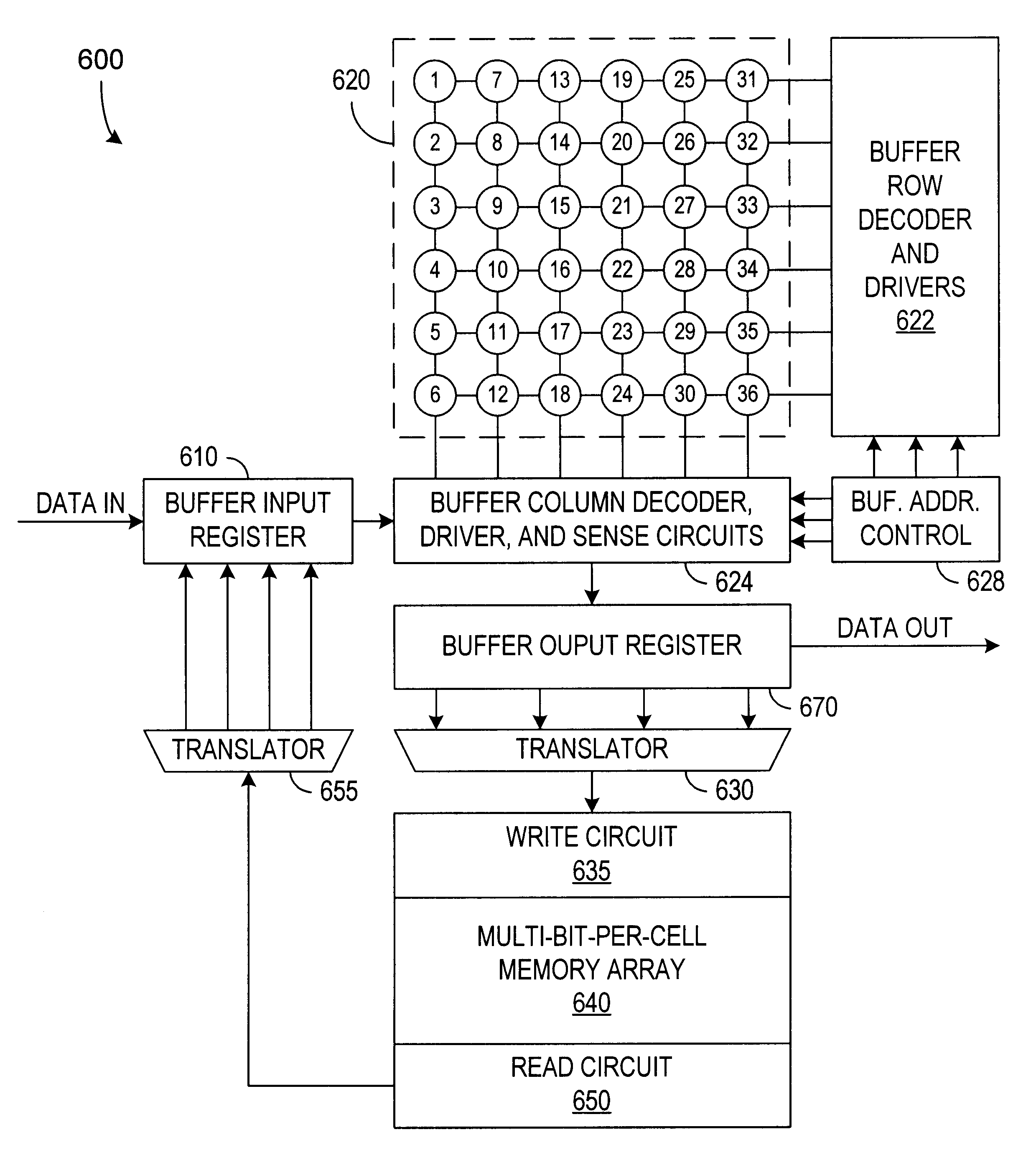
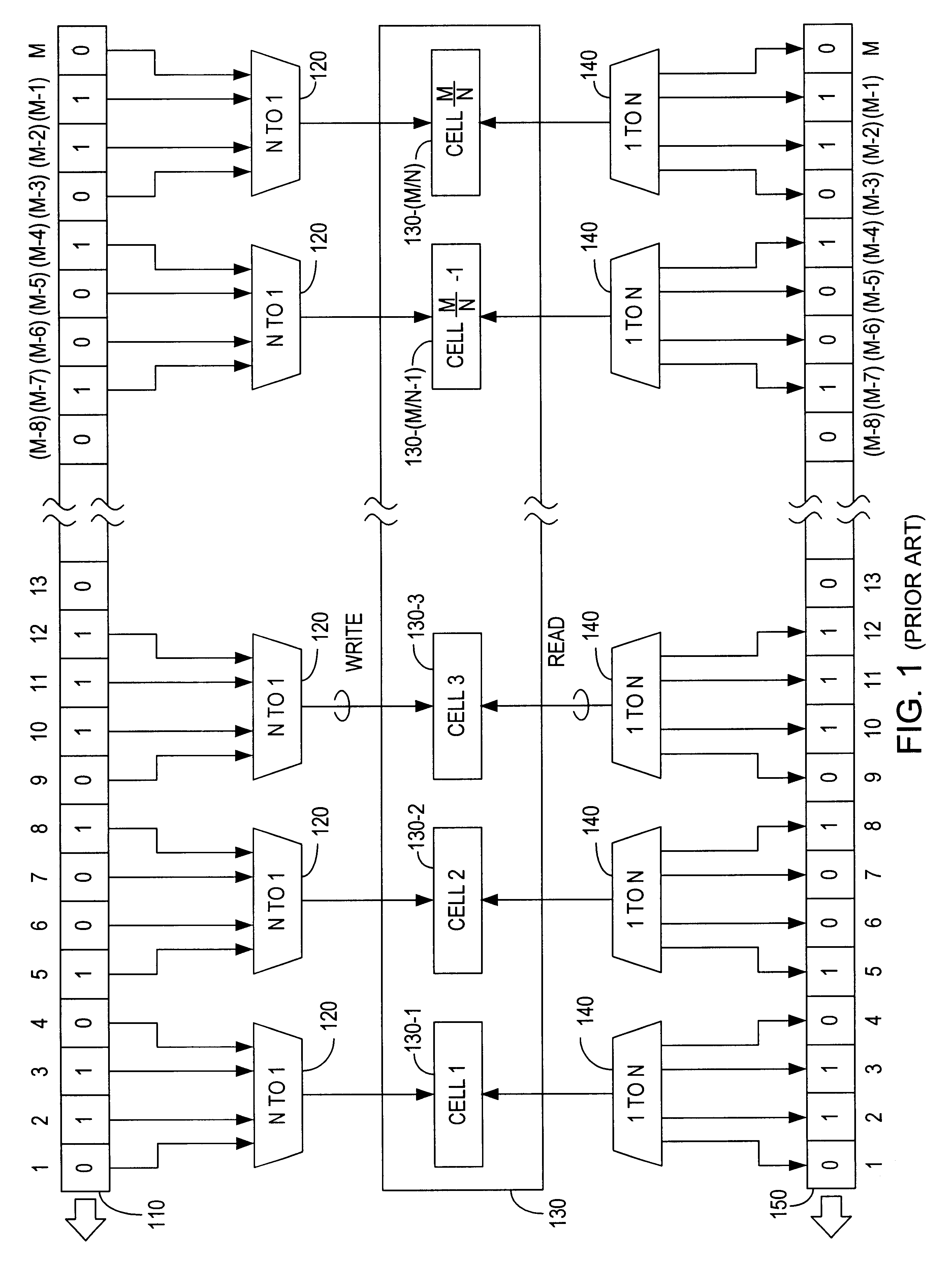
    Densbits Technologies Ltd. · December 18, 2012

  158. US9104550B2

    Physical levels deterioration based determination of thresholds useful for converting cell physical levels into cell logical values in an array of digital memory cells

    Densbits Technologies Ltd. · August 11, 2015

  159. US8321625B2

    Flash memory device with physical cell value deterioration accommodation and methods useful in conjunction therewith

    Densbits Technologies Ltd. · November 27, 2012

  160. US20100131831A1

    low power chien-search based bch/rs decoding system for flash memory, mobile communications devices and other applications

    Hanan Weingarten · May 27, 2010 · Examiner cited

  161. US20100146191A1

    System and methods employing mock thresholds to generate actual reading thresholds in flash memory devices

    Michael Katz · June 10, 2010 · Examiner cited

  162. US8627188B2

    Flash memory apparatus and methods using a plurality of decoding stages including optional use of concatenated BCH codes and/or designation of “first below” cells
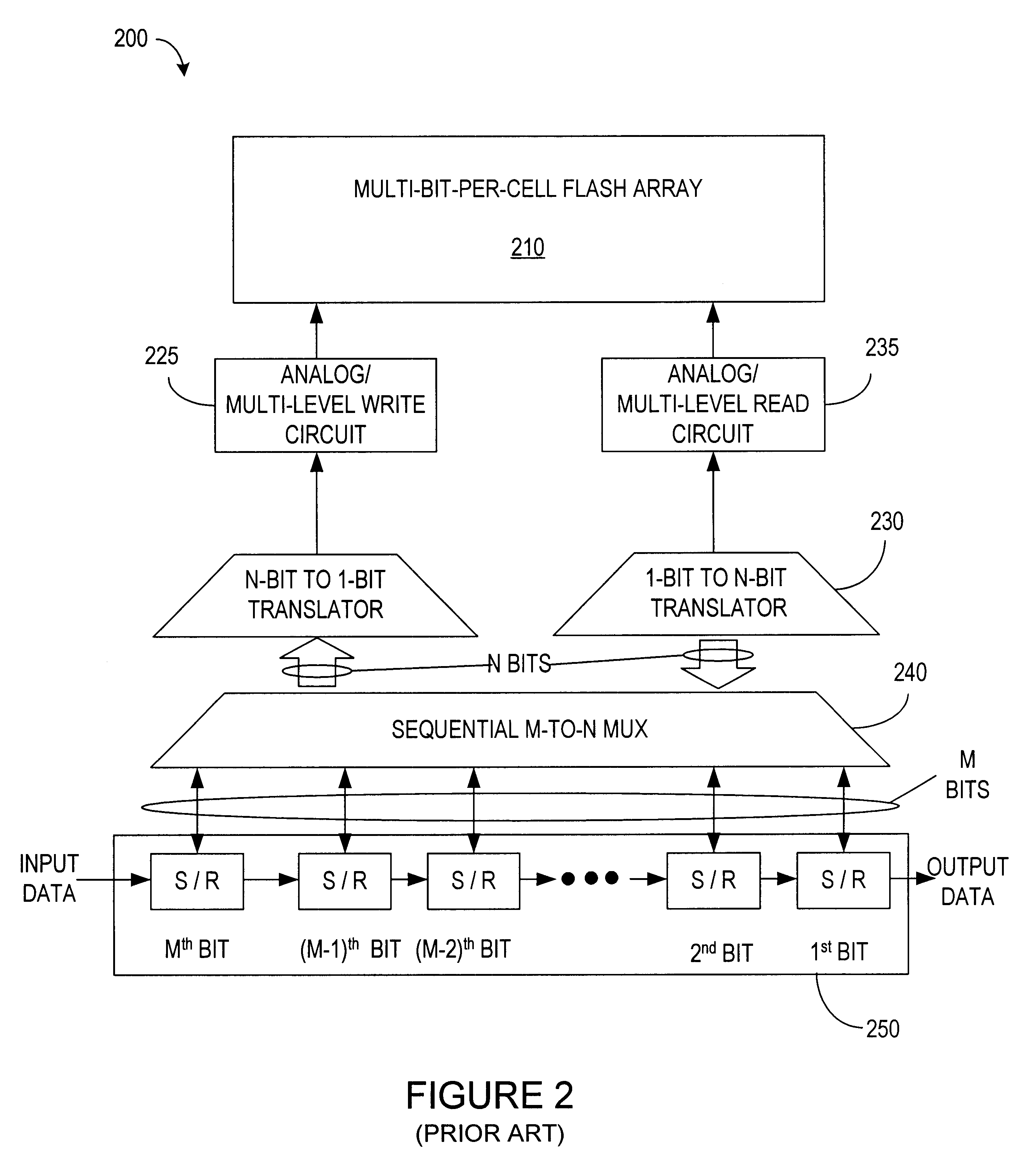
    Densbits Technologies Ltd. · January 7, 2014

  163. US8341335B2

    Flash memory apparatus with a heating system for temporarily retired memory portions

    Densbits Technologies Ltd. · December 25, 2012

  164. US8453022B2

    Apparatus and methods for generating row-specific reading thresholds in flash memory

    Densbits Technologies Ltd. · May 28, 2013

  165. US8843698B2

    Systems and methods for temporarily retiring memory portions

    Densbits Technologies Ltd. · September 23, 2014

  166. US8751726B2

    System and methods employing mock thresholds to generate actual reading thresholds in flash memory devices

    Densbits Technologies Ltd. · June 10, 2014

  167. US8607128B2

    Low power chien-search based BCH/RS decoding system for flash memory, mobile communications devices and other applications

    Densbits Technologies Ltd. · December 10, 2013

  168. US8782500B2

    Systems and methods for error correction and decoding on multi-level physical media

    Densbits Technologies Ltd. · July 15, 2014

  169. US8209588B2

    Efficient interference cancellation in analog memory cell arrays

    Anobit Technologies Ltd. · June 26, 2012

  170. US20090158126A1

    Efficient interference cancellation in analog memory cell arrays

    Anobit Technologies Ltd · June 18, 2009 · Examiner cited

  171. US8359516B2

    Systems and methods for error correction and decoding on multi-level physical media

    Densbits Technologies Ltd. · January 22, 2013

  172. US8276051B2

    Chien-search system employing a clock-gating scheme to save power for error correction decoder and other applications

    Densbits Technologies Ltd. · September 25, 2012

  173. US8456905B2

    Efficient data storage in multi-plane memory devices

    Apple Inc. · June 4, 2013

  174. US8327246B2

    Apparatus for coding at a plurality of rates in multi-level flash memory systems, and methods useful in conjunction therewith

    Densbits Technologies Ltd. · December 4, 2012

  175. US20090168524A1

    Wear level estimation in analog memory cells

    Anobit Technologies Ltd. · July 2, 2009 · Examiner cited

  176. US8085586B2

    Wear level estimation in analog memory cells

    Anobit Technologies Ltd. · December 27, 2011

  177. US8762800B1

    Systems and methods for handling immediate data errors in flash memory

    Densbits Technologies Ltd. · June 24, 2014

  178. US20090199074A1

    Parameter estimation based on error correction code parity check equations

    Anobit Technologies Ltd. · August 6, 2009 · Examiner cited

  179. US8156398B2

    Parameter estimation based on error correction code parity check equations

    Anobit Technologies Ltd. · April 10, 2012

  180. US7924587B2

    Programming of analog memory cells using a single programming pulse per state transition

    Anobit Technologies Ltd. · April 12, 2011

  181. US20090213653A1

    Programming of analog memory cells using a single programming pulse per state transition

    Anobit Technologies Ltd · August 27, 2009 · Examiner cited

  182. US7864573B2

    Programming analog memory cells for reduced variance after retention

    Anobit Technologies Ltd. · January 4, 2011

  183. US20090228761A1

    Efficient readout from analog memory cells using data compression

    Anobit Technologies Ltd · September 10, 2009 · Examiner cited

  184. US8230300B2

    Efficient readout from analog memory cells using data compression

    Apple Inc. · July 24, 2012

  185. US20090235145A1

    Memory device repair apparatus, systems, and methods

    Micron Technology, Inc. · September 17, 2009 · Examiner cited

  186. US8694861B2

    Memory device repair apparatus, systems, and methods

    Micron Technology, Inc. · April 8, 2014

  187. US8255771B2

    Memory device repair apparatus, systems, and methods

    Micron Technology, Inc. · August 28, 2012 · Examiner cited

  188. US8400858B2

    Memory device with reduced sense time readout

    Apple Inc. · March 19, 2013

  189. US8059457B2

    Memory device with multiple-accuracy read commands

    Anobit Technologies Ltd. · November 15, 2011

  190. US20090240872A1

    Memory device with multiple-accuracy read commands

    Anobit Technologies Ltd · September 24, 2009 · Examiner cited

  191. US20100131580A1

    Apparatus and methods for hardware-efficient unbiased rounding

    Densbits Technologies Ltd. · May 27, 2010 · Examiner cited

  192. US8972472B2

    Apparatus and methods for hardware-efficient unbiased rounding

    Densbits Technologies Ltd. · March 3, 2015

  193. US8498151B1

    Data storage in analog memory cells using modified pass voltages

    Apple Inc. · July 30, 2013

  194. US7995388B1

    Data storage using modified voltages

    Anobit Technologies Ltd. · August 9, 2011

  195. US7924613B1

    Data storage in analog memory cells with protection against programming interruption

    Anobit Technologies Ltd. · April 12, 2011

  196. US8332725B2

    Reprogramming non volatile memory portions

    Densbits Technologies Ltd. · December 11, 2012

  197. US8949684B1

    Segmented data storage

    Apple Inc. · February 3, 2015

  198. US8169825B1

    Reliable data storage in analog memory cells subjected to long retention periods

    Anobit Technologies Ltd. · May 1, 2012

  199. US8145855B2

    Built in on-chip data scrambler for non-volatile memory

    Sandisk Technologies Inc. · March 27, 2012

  200. USRE45515E1

    Built in on-chip data scrambler for non-volatile memory

    Sandisk Technologies Inc. · May 12, 2015

  201. US20100070681A1

    Method for scrambling data in which scrambling data and scrambled data are stored in corresponding non-volatile memory locations

    Jun Wan · March 18, 2010 · Examiner cited

  202. US8429330B2

    Method for scrambling data in which scrambling data and scrambled data are stored in corresponding non-volatile memory locations

    Sandisk Technologies Inc. · April 23, 2013

  203. US20100070682A1

    Built in on-chip data scrambler for non-volatile memory

    Jun Wan · March 18, 2010 · Examiner cited

  204. US8482978B1

    Estimation of memory cell read thresholds by sampling inside programming level distribution intervals

    Apple Inc. · July 9, 2013

  205. US8000135B1

    Estimation of memory cell read thresholds by sampling inside programming level distribution intervals

    Anobit Technologies Ltd. · August 16, 2011

  206. US8239734B1

    Efficient data storage in storage device arrays

    Apple Inc. · August 7, 2012

  207. US20110069548A1

    Data path for multi-level cell memory, methods for storing and methods for utilizing a memory array

    Micron Technology, Inc. · March 24, 2011 · Examiner cited

  208. US7852671B2

    Data path for multi-level cell memory, methods for storing and methods for utilizing a memory array

    Micron Technology, Inc. · December 14, 2010

  209. US8787081B2

    Data path for multi-level cell memory, methods for storing and methods for utilizing a memory array

    Micron Technology, Inc. · July 22, 2014

  210. TWI424442B

    Data path for multi-level cell memory, methods for storing and methods for utilizing a memory array

    Micron Technology Inc · January 21, 2014 · Examiner cited

  211. US8374027B2

    Data path for multi-level cell memory, methods for storing and methods for utilizing a memory array

    Micron Technology, Inc. · February 12, 2013

  212. JP2012507819A

    Data path, storage method and memory array usage for multi-level cell memory

    マイクロン テクノロジー, インク. · March 29, 2012 · Examiner cited

  213. US8482979B2

    Data path for multi-level cell memory, methods for storing and methods for utilizing a memory array

    Micron Technology, Inc. · July 9, 2013

  214. US20100110788A1

    Data path for multi-level cell memory, methods for storing and methods for utilizing a memory array

    Micron Technology, Inc. · May 6, 2010 · Examiner cited

  215. WO2010096099A1

    Data path for multi-level cell memory, methods for storing and methods for utilizing a memory array

    Micron Technology, Inc. · August 26, 2010

  216. US8261159B1

    Data scrambling schemes for memory devices

    Apple, Inc. · September 4, 2012

  217. EP2351039B1

    Data path for multi-level cell memory, methods for storing and methods for utilizing a memory array

    Micron Technology, Inc. · December 30, 2020 · Examiner cited

  218. US8208304B2

    Storage at M bits/cell density in N bits/cell analog memory cell devices, M>N

    Anobit Technologies Ltd. · June 26, 2012

  219. US20100124088A1

    Storage at m bits/cell density in n bits/cell analog memory cell devices, m>n

    Anobit Technologies Ltd · May 20, 2010 · Examiner cited

  220. US20100165689A1

    Rejuvenation of analog memory cells

    Anobit Technologies Ltd · July 1, 2010 · Examiner cited

  221. US8397131B1

    Efficient readout schemes for analog memory cell devices

    Apple Inc. · March 12, 2013

  222. US8174857B1

    Efficient readout schemes for analog memory cell devices using multiple read threshold sets

    Anobit Technologies Ltd. · May 8, 2012

  223. US8248831B2

    Rejuvenation of analog memory cells

    Apple Inc. · August 21, 2012

  224. US8924661B1

    Memory system including a controller and processors associated with memory devices

    Apple Inc. · December 30, 2014

  225. US8228701B2

    Selective activation of programming schemes in analog memory cell arrays

    Apple Inc. · July 24, 2012

  226. US20100250836A1

    Use of Host System Resources by Memory Controller

    Anobit Technologies Ltd · September 30, 2010 · Examiner cited

  227. US8259506B1

    Database of memory read thresholds

    Apple Inc. · September 4, 2012

  228. US8832354B2

    Use of host system resources by memory controller

    Apple Inc. · September 9, 2014

  229. US8458574B2

    Compact chien-search based decoding apparatus and method

    Densbits Technologies Ltd. · June 4, 2013

  230. US8850296B2

    Encoding method and system, decoding method and system

    Densbits Technologies Ltd. · September 30, 2014

  231. US8819385B2

    Device and method for managing a flash memory

    Densbits Technologies Ltd. · August 26, 2014

  232. US20100253555A1

    Encoding method and system, decoding method and system

    Hanan Weingarten · October 7, 2010 · Examiner cited

  233. US8238157B1

    Selective re-programming of analog memory cells

    Apple Inc. · August 7, 2012

  234. US8566510B2

    Systems and method for flash memory management

    Densbits Technologies Ltd. · October 22, 2013

  235. US8479080B1

    Adaptive over-provisioning in memory systems

    Apple Inc. · July 2, 2013

  236. US20110051521A1

    Flash memory module and method for programming a page of flash memory cells

    Shmuel Levy · March 3, 2011 · Examiner cited

  237. US8995197B1

    System and methods for dynamic erase and program control for flash memory device memories

    Densbits Technologies Ltd. · March 31, 2015

  238. US9330767B1

    Flash memory module and method for programming a page of flash memory cells

    Avago Technologies General Ip (Singapore) Pte. Ltd. · May 3, 2016

  239. US8305812B2

    Flash memory module and method for programming a page of flash memory cells

    Densbits Technologies Ltd. · November 6, 2012

  240. US8868821B2

    Systems and methods for pre-equalization and code design for a flash memory

    Densbits Technologies Ltd. · October 21, 2014

  241. US8730729B2

    Systems and methods for averaging error rates in non-volatile devices and storage systems

    Densbits Technologies Ltd. · May 20, 2014

  242. US8495465B1

    Error correction coding over multiple memory pages

    Apple Inc. · July 23, 2013

  243. US8724387B2

    Method, system, and computer readable medium for reading and programming flash memory cells using multiple bias voltages

    Densbits Technologies Ltd. · May 13, 2014

  244. US8626988B2

    System and method for uncoded bit error rate equalization via interleaving

    Densbits Technologies Ltd. · January 7, 2014

  245. US20110119562A1

    System and method for uncoded bit error rate equalization via interleaving

    Steiner Avi · May 19, 2011 · Examiner cited

  246. US8677054B1

    Memory management schemes for non-volatile memory devices

    Apple Inc. · March 18, 2014

  247. US9037777B2

    Device, system, and method for reducing program/read disturb in flash arrays

    Densbits Technologies Ltd. · May 19, 2015

  248. US20110153919A1

    Device, system, and method for reducing program/read disturb in flash arrays

    Erez Sabbag · June 23, 2011 · Examiner cited

  249. US8607124B2

    System and method for setting a flash memory cell read threshold

    Densbits Technologies Ltd. · December 10, 2013

  250. US20110161775A1

    System and method for setting a flash memory cell read threshold

    Hanan Weingarten · June 30, 2011 · Examiner cited

  251. US8694814B1

    Reuse of host hibernation storage space by memory controller

    Apple Inc. · April 8, 2014

  252. US8677203B1

    Redundant data storage schemes for multi-die memory systems

    Apple Inc. · March 18, 2014

  253. US8572311B1

    Redundant data storage in multi-die memory systems

    Apple Inc. · October 29, 2013

  254. US20110214039A1

    System and method for multi-dimensional decoding

    Steiner Avi · September 1, 2011 · Examiner cited

  255. US8700970B2

    System and method for multi-dimensional decoding

    Densbits Technologies Ltd. · April 15, 2014

  256. US8341502B2

    System and method for multi-dimensional decoding

    Densbits Technologies Ltd. · December 25, 2012

  257. US20110214029A1

    System and method for multi-dimensional decoding

    Steiner Avi · September 1, 2011 · Examiner cited

  258. US8527840B2

    System and method for restoring damaged data programmed on a flash device

    Densbits Technologies Ltd. · September 3, 2013

  259. US8516274B2

    Method, system and medium for analog encryption in a flash memory

    Densbits Technologies Ltd. · August 20, 2013

  260. US9104610B2

    Method, system and medium for analog encryption in a flash memory

    Densbits Technologies Ltd. · August 11, 2015

  261. US8745317B2

    System and method for storing information in a multi-level cell memory

    Densbits Technologies Ltd. · June 3, 2014

  262. US9021177B2

    System and method for allocating and using spare blocks in a flash memory

    Densbits Technologies Ltd. · April 28, 2015

  263. US8694853B1

    Read commands for reading interfering memory cells

    Apple Inc. · April 8, 2014

  264. US20110289278A1

    Method of estimating read level for a memory device, memory controller therefor, and recording medium

    Eun Hee Seok · November 24, 2011 · Examiner cited

  265. US8516183B2

    Method of estimating read level for a memory device, memory controller therefor, and recording medium

    Samsung Electronics Co., Ltd. · August 20, 2013 · Examiner cited

  266. US8572423B1

    Reducing peak current in memory systems

    Apple Inc. · October 29, 2013

  267. US8539311B2

    System and method for data recovery in multi-level cell memories

    Densbits Technologies Ltd. · September 17, 2013

  268. US8850297B1

    System and method for multi-dimensional encoding and decoding

    Densbits Technologies Ltd. · September 30, 2014

  269. US8510639B2

    System and method for multi-dimensional encoding and decoding

    Densbits Technologies Ltd. · August 13, 2013

  270. US8621321B2

    System and method for multi-dimensional encoding and decoding

    Densbits Technologies Ltd. · December 31, 2013

  271. US8468431B2

    System and method for multi-dimensional encoding and decoding

    Densbits Technologies Ltd. · June 18, 2013

  272. US8467249B2

    Systems and methods for storing, retrieving, and adjusting read thresholds in flash memory storage system

    Densbits Technologies Ltd. · June 18, 2013

  273. US8595591B1

    Interference-aware assignment of programming levels in analog memory cells

    Apple Inc. · November 26, 2013

  274. US9104580B1

    Cache memory for hybrid disk drives

    Apple Inc. · August 11, 2015

  275. US8767459B1

    Data storage in analog memory cells across word lines using a non-integer number of bits per cell

    Apple Inc. · July 1, 2014

  276. US8645794B1

    Data storage in analog memory cells using a non-integer number of bits per cell

    Apple Inc. · February 4, 2014

  277. US8856475B1

    Efficient selection of memory blocks for compaction

    Apple Inc. · October 7, 2014

  278. US8694854B1

    Read threshold setting based on soft readout statistics

    Apple Inc. · April 8, 2014

  279. US8964464B2

    System and method for accelerated sampling

    Densbits Technologies Ltd. · February 24, 2015

  280. US8508995B2

    System and method for adjusting read voltage thresholds in memories

    Densbits Technologies Ltd. · August 13, 2013

  281. US9021181B1

    Memory management for unifying memory cell conditions by using maximum time intervals

    Apple Inc. · April 28, 2015

  282. US9063878B2

    Method, system and computer readable medium for copy back

    Densbits Technologies Ltd. · June 23, 2015

  283. US8850100B2

    Interleaving codeword portions between multiple planes and/or dies of a flash memory device

    Densbits Technologies Ltd. · September 30, 2014

  284. US10079068B2

    Devices and method for wear estimation based memory management

    Avago Technologies General Ip (Singapore) Pte. Ltd. · September 18, 2018

  285. US8693258B2

    Obtaining soft information using a hard interface

    Densbits Technologies Ltd. · April 8, 2014

  286. US8990665B1

    System, method and computer program product for joint search of a read threshold and soft decoding

    Densbits Technologies Ltd. · March 24, 2015

  287. US9195592B1

    Advanced management of a non-volatile memory

    Densbits Technologies Ltd. · November 24, 2015

  288. US9372792B1

    Advanced management of a non-volatile memory

    Avago Technologies General Ip (Singapore) Pte. Ltd. · June 21, 2016

  289. US9396106B2

    Advanced management of a non-volatile memory

    Avago Technologies General Ip (Singapore) Pte. Ltd. · July 19, 2016

  290. US8996790B1

    System and method for flash memory management

    Densbits Technologies Ltd. · March 31, 2015

  291. US9110785B1

    Ordered merge of data sectors that belong to memory space portions

    Densbits Technologies Ltd. · August 18, 2015

  292. US9501392B1

    Management of a non-volatile memory module

    Avago Technologies General Ip (Singapore) Pte. Ltd. · November 22, 2016

  293. US8667211B2

    System and method for managing a non-volatile memory

    Densbits Technologies Ltd. · March 4, 2014

  294. US8588003B1

    System, method and computer program product for programming and for recovering from a power failure

    Densbits Technologies Ltd. · November 19, 2013

  295. US8553468B2

    System and method for managing erase operations in a non-volatile memory

    Densbits Technologies Ltd. · October 8, 2013

  296. US8996788B2

    Configurable flash interface

    Densbits Technologies Ltd. · March 31, 2015

  297. US8947941B2

    State responsive operations relating to flash memory cells

    Densbits Technologies Ltd. · February 3, 2015

  298. US8976584B2

    Flash memory device and method of programming the same

    Samsung Electronics Co., Ltd. · March 10, 2015

  299. US8996793B1

    System, method and computer readable medium for generating soft information

    Densbits Technologies Ltd. · March 31, 2015

  300. US8838937B1

    Methods, systems and computer readable medium for writing and reading data

    Densbits Technologies Ltd. · September 16, 2014

  301. US8879325B1

    System, method and computer program product for processing read threshold information and for reading a flash memory module

    Densbits Technologies Ltd. · November 4, 2014

  302. US9431118B1

    System, method and computer program product for processing read threshold information and for reading a flash memory module

    Avago Technologies General Ip (Singapore) Pte. Ltd. · August 30, 2016

  303. US9921954B1

    Method and system for split flash memory management between host and storage controller

    Avago Technologies General Ip (Singapore) Pte. Ltd. · March 20, 2018

  304. US9368225B1

    Determining read thresholds based upon read error direction statistics

    Avago Technologies General Ip (Singapore) Pte. Ltd. · June 14, 2016

  305. US9069659B1

    Read threshold determination using reference read threshold

    Densbits Technologies Ltd. · June 30, 2015

  306. US9136876B1

    Size limited multi-dimensional decoding

    Densbits Technologies Ltd. · September 15, 2015

  307. US9413491B1

    System and method for multiple dimension decoding and encoding a message

    Avago Technologies General Ip (Singapore) Pte. Ltd. · August 9, 2016

  308. US9348694B1

    Detecting and managing bad columns

    Avago Technologies General Ip (Singapore) Pte. Ltd. · May 24, 2016

  309. US9397706B1

    System and method for irregular multiple dimension decoding and encoding

    Avago Technologies General Ip (Singapore) Pte. Ltd. · July 19, 2016

  310. US9786388B1

    Detecting and managing bad columns

    Avago Technologies General Ip (Singapore) Pte. Ltd. · October 10, 2017

  311. US9536612B1

    Digital signaling processing for three dimensional flash memory arrays

    Avago Technologies General Ip (Singapore) Pte. Ltd · January 3, 2017

  312. US10120792B1

    Programming an embedded flash storage device

    Avago Technologies General Ip (Singapore) Pte. Ltd. · November 6, 2018

  313. US9542262B1

    Error correction

    Avago Technologies General Ip (Singapore) Pte. Ltd. · January 10, 2017

  314. US9892033B1

    Management of memory units

    Avago Technologies General Ip (Singapore) Pte. Ltd. · February 13, 2018

  315. US9584159B1

    Interleaved encoding

    Avago Technologies General Ip (Singapore) Pte. Ltd. · February 28, 2017

  316. US9407291B1

    Parallel encoding method and system

    Avago Technologies General Ip (Singapore) Pte. Ltd. · August 2, 2016

  317. US9972393B1

    Accelerating programming of a flash memory module

    Avago Technologies General Ip (Singapore) Pte. Ltd. · May 15, 2018

  318. US9449702B1

    Power management

    Avago Technologies General Ip (Singapore) Pte. Ltd. · September 20, 2016

  319. WO2016018299A1

    Split memory bank

    Hewlett-Packard Development Company, L.P. · February 4, 2016 · Examiner cited

  320. US10014055B2

    Split memory bank

    Hewlett-Packard Development Company, L.P. · July 3, 2018

  321. US10403362B2

    Split memory bank

    Hewlett-Packard Development Company, L.P. · September 3, 2019

  322. US10236063B2

    Split memory bank

    Hewlett-Packard Development Company, L.P. · March 19, 2019

  323. US9524211B1

    Codeword management

    Avago Technologies General Ip (Singapore) Pte. Ltd. · December 20, 2016

  324. US10305515B1

    System and method for encoding using multiple linear feedback shift registers

    Avago Technologies International Sales Pte. Limited · May 28, 2019

  325. US10628255B1

    Multi-dimensional decoding

    Avago Technologies International Sales Pte. Limited · April 21, 2020

  326. US9851921B1

    Flash memory chip processing

    Avago Technologies General Ip (Singapore) Pte. Ltd. · December 26, 2017

  327. US10558585B2

    Dynamic memory scrambling

    Arm Limited · February 11, 2020 · Examiner cited

  328. US9954558B1

    Fast decoding of data stored in a flash memory

    Avago Technologies General Ip (Singapore) Pte. Ltd. · April 24, 2018

  329. US20200028856A1

    Port scrambling usage in heterogeneous networks

    Cyber 2.0 (2015) LTD · January 23, 2020 · Examiner cited

  330. WO2020028120A1

    Data protection in computer processors

    Micron Technology, Inc. · February 6, 2020 · Examiner cited

  331. US11113422B2

    Data protection in computer processors

    Micron Technology, Inc. · September 7, 2021

  332. US11914756B2

    Data protection in computer processors

    Micron Technology, Inc. · February 27, 2024

  333. US11556416B2

    Controlling memory readout reliability and throughput by adjusting distance between read thresholds

    Apple Inc. · January 17, 2023

  334. US11847342B2

    Efficient transfer of hard data and confidence levels in reading a nonvolatile memory

    Apple Inc. · December 19, 2023

  335. US12007439B1

    Method and apparatus for integrated circuit testing

    Winbond Electronics Corp. · June 11, 2024 · Examiner cited

Related Patents